

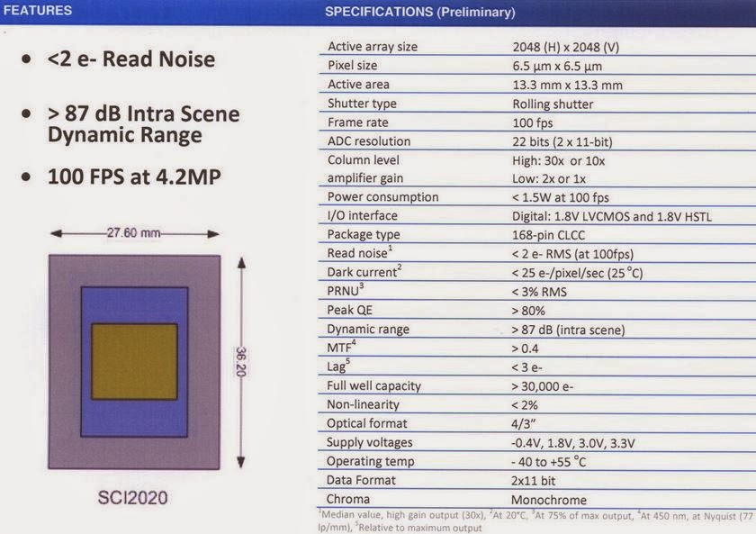

My first impressions:
- 3% RMS PRNU is quite high for such a large pixel. Not clear why it's that high.
- 30,000e- full well over 2e- read noise does not make 87db DR, like the table states. May be achieved at slower speeds when the read noise is lower
- -0.4V supply voltage is used for Tx gate bias during integration, I guess.
Thanks to BP for the info!
I think 87dB is what you get by combining the output from the two parallel readout circuits.
ReplyDeleteWhatever the parallel readout paths are, their combined DR can't exceed that of pixel.
DeleteVladimir, what could be the capacitance of the FD in the pixel according to your feeling please ?
Delete-yang ni
3-4fF, if I have to guess.
DeleteOne channel applies a bigger gain without increasing the read-out noise, then the camera maker has to mix the signal from the two channels to get an image with detail both in the highlights and the shadows.
DeleteThe sCMOS v1 had a full well capacity of 30000 e-, read-out noise of 2e- at 30fps and 3e- at 100 fps, and it did reach (as seen on the BlackMagic cameras) the 88dB of DR that they claimed. For the record, QEmax 60%.
Some info on the sCMOS v1:
http://www.andor.com/learning-academy/dual-amplifier-dynamic-range-scmos-dynamic-range
http://www.pco.de/whats-new/high-dynamic-range-imaging-with-scmos-scientific-cmos/
http://www.pco.de/fileadmin/user_upload/db/download/scmos_white_paper_2mb_01.pdf
So, for the high gain channel, the noise is 2e-, limited by the pixel, no matter how low the readout channel noise is. And for the low gain channel, the full well is 30,000e-, again limited by the pixel, even if the readout could manage a much larger signal. How do we get the 87db DR then?
DeleteDR=20log(30000e/2e)=83.5dB. You can have 32 bit ADC, whatever..it would not change that, unless you use multiple exposures, LOFIC, or logarithmic (3T kind) pixel which doesn't seem to be the case here..
DeleteWell, no idea then. As I said, I'm not an expert. I was just drinking their kool-aid and passing it on
DeleteHamamatsu, on this Page: http://thelivingimage.hamamatsu.com/resources/will-able-differentiate-1500-molecules-1475-whats-dynamic-range/ says "Using the Orca Flash 4.0 as an example, we divide the full well capacity of 30,000 electrons by the read noise at slow scan, which is 0.9 electrons, to get a dynamic range of 33,000:1, or 90.37 dB." (dB corrected by me)
DeleteOn Page 8 Andor explains this technique: http://www.andor.com/pdfs/literature/Andor_sCMOS_Brochure.pdf
"
The Andor Neo and Zyla cameras are designed to make use of the innovative dual
‘column-level’ amplifier design of the sensors.
Traditionally, sensors require that the user must select up-front between high or low amplifier gain (i.e. sensitivity) settings, depending on whether they want to optimize for low noise or maximum well depth. The dual amplifier architecture of the sCMOS sensor circumvents this need, in that signal can be sampled simultaneously by both high and low gain amplifiers. As such, the lowest noise of the chip can be harnessed alongside the maximum well depth, affording widest possible dynamic range of up to 33,000:1.
".
The transition point (between the choice of low or high gain on each pixel) is calculated by an FPGA and the two imaged are merged.
An even longer Technical Note appears on Page 19 of Andor's PDF, along with a Diagram of the Circuit. That gives a more complete answer.
With 11bits in the ADC is not possible to codify a dynamic range higher than 77dB. Only if some non linear transform is used can be codified
ReplyDeleteThey have an equivalent of two 11b ADCs with different gains combined. This gives them a higher DR.
Deletea couple of definition issues:
ReplyDelete-22bit ADC is a wrong notation. They could claim max 16bit (11bit adc + 5bits from the gain of 32 of the gain amplifier).
-3% PRNU seems high. That limits the max SNR to 30dB(?). Please correct me if I'm wrong
You are correct, if there is no PRNU correction you are limited at ~30dB.
DeleteDR is probably for the pixel, so PRNU is not included.
Delete2e noise is for 100fps. The noise at 30fps may be 1e and then DR=87dB. This is possible as the dark current related shot noise for lower fps is only slightly higher: sqrt(25e/30).
This is a polished good old 4T pixel sensor.
No price? :)
ReplyDeleteVladimir, how can you guess the TX voltage is -0.4V during integration period ?
ReplyDeleteThanks !
-yang ni
I just do not see any other need for this negative supply in their spec.
Deleteah ! I didn't notice that ! Thanks !
Delete-yang ni
Is there any reason for the square resolution? Is this common in scientific cameras? Thanks!
ReplyDeleteit's quite optimal for optical system where you have an fully corrected imaging circle of given size and you want to get max of that circle.
DeleteThis seems very similar to the version 2 scmos sensor that Hamamatsu released a year ago. Could it be the same sensor?
ReplyDelete