Link: https://www.prophesee.ai/2026/06/15/prophesee-launches-mantara-event-based-drone-detection/
Prophesee raises €20 million and launches Mantara, the first fully integrated drone detection system built on event-based vision and AI
PARIS, June 15, 2026 – As Eurosatory and Vivatech open their doors this week in Paris, Prophesee – inventor and world leader in event-based perception – announces the launch of Mantara®: the first integrated system built natively event-based for drone detection and tracking. Mantara runs on Hearth®, a new software platform with built-in AI processing.
Field-validated in June 2026, Mantara is powered by Hearth, the platform succeeding OpenEB and the Metavision SDK. These announcements coincide with a €20 million capital raise led by French fund Critical Path Ventures, with participation from existing shareholders. Prophesee is now held by a substantial majority of French shareholders.
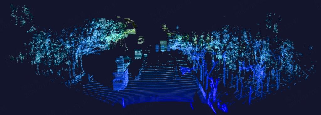
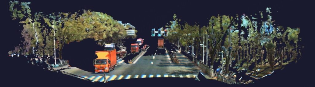
Mantara is a camera whose performance rests on integrated sensors that do not capture images but motion and events. Each pixel responds independently, in microseconds, the instant movement occurs. Fast, erratic targets that blur or vanish between frames on a conventional camera remain perfectly visible and fully characterizable by Mantara: in low light, in backlit conditions, against cluttered backgrounds. Low latency is the heart of its edge: in the time a conventional system takes to capture, transfer, and process a single frame, Mantara has already detected a drone, characterized it, and triggered a response or initiated tracking.
This capability is rooted in a bio-mimetic design inspired by the human visual system. The eye does not record the world in full. Instead, it captures sparse, essential signals, and the brain reconstructs and interprets what matters. If Mantara is the eye, Hearth is the brain.
Hearth is built with cybersecurity requirements, GDPR compliance, and AI governance standards baked in. It enables sensor fusion and will ensure backward compatibility across successive generations of Prophesee sensors. Applications built on Metavision and OpenEB will migrate to Hearth seamlessly.
Recent conflicts have put drones at the center of modern warfare, and the threat is moving fast beyond the battlefield: airports, power plants, critical infrastructure, public gatherings. Drones fly low, change direction sharply, and increasingly carry a near-zero signature: minimal electromagnetic emissions, little acoustic output, little thermal trace. They arrive faster, and in greater numbers, with coordinated swarms capable of overwhelming defenses built to track a single target.
Mantara emits nothing. It cannot be detected or jammed. And it learns: Hearth delivers regular updates that allow every deployed unit to adapt to shifts in threat behavior. Ukraine has made this clear: tactics evolve far faster than traditional development cycles can follow.
Civil and Military Missions
Mantara serves both civil and defense use cases. Airports, stadiums, energy and industrial sites, prisons, and ports can integrate it into existing security infrastructure for continuous, automated airspace monitoring. Governments and defense organizations have access to the same system for force protection and counter-UAS operations.
For civil operators, Mantara also offers a compelling privacy advantage: because the sensors detect motion events rather than recording images, Mantara can track moving objects without ever producing footage that could identify individuals. This is a decisive asset for deployment over public spaces and for GDPR compliance.
Hearth: the Reference Platform for the Event-based Ecosystem
Mantara is part of a broader strategic shift encompassing Prophesee’s entire product line.
Hearth will give the event-based ecosystem a trusted reference environment for building scalable, production-grade modules and applications. It will manage sensor updates, backward compatibility, and unlock capabilities that were previously out of reach for developers and integrators working with Prophesee’s patented technology.
As part of this transition, Prophesee announces the end of life of OpenEB, its open-source framework, and of the standalone Metavision SDK. Hearth is the path forward for the developer community. Prophesee will support the migration.
Prophesee’s partners and customers have built a wide range of applications – from eye trackers and ADAS (Advanced Driver Assistance Systems) to ultra-fast cameras for smartphones, ping-pong playing robots, industrial inspection systems, and drone and satellite tracking and targeting solutions. Event-based vision is reaching an inflection point. The market is maturing rapidly and demanding solutions that are robust, secure, and production-ready. With around a hundred patents and multiple sensors to its name, Prophesee has industrialized event-based technology and now intends to structure the broader application ecosystem by making Hearth widely available.
Built with a Network of European Industrial Partners
Mantara benefits from Prophesee’s partnership with IDS Imaging Development Systems GmbH, a leading industrial camera manufacturer. Building on the commercial success of the IDS uEye EVS camera line – based on Prophesee sensors – the two companies expanded their partnership in March 2026 with an agreement signed at Embedded World in Nuremberg to co-develop next-generation industrial vision systems.
Prophesee and Exosens have entered an MoU, paving the way for a long-term partnership to extend bio-mimetic technology beyond the visible spectrum, combining Prophesee’s event-based vision with Exosens’ detection and imaging technologies.
A €20 Million Raise to Anchor Prophesee in France
Prophesee announces a €20 million capital raise led by Critical Path Ventures, a new investor. The team has been reinforced with talent from Google, Microsoft, BCG, Thales, and companies working in drone, robotics, and quantum technologies, as well as from the armed forces. The funds will support the commercial scale-up of Mantara, the development of embedded intelligence within sensors, and the launch of Hearth.