Monday, January 31, 2022

Hynix Begins Mass Production of 0.7um Pixels

BusinessKorea: Keeping an earlier promise, SK Hynix has started to mass-production of 50MP sensors with 0.7㎛ pixels. The image quality is said to be "at the same level as Sony products."

Samsung has been manufacturing a 50MP sensor with 0.64㎛ pixels since June 2021. Omnivision announced 200MP sensor with 0.61㎛ pixels.

SK Hynix is expected to supply its 50MP 0.7um sensor to Samsung for use in Galaxy A series of smartphones scheduled to be released in the 2H2021. Previously, SK Hynix supplied 1.0㎛ pixel-based 13MP sensors for Samsung's foldable smartphone Galaxy Z Flip 3.

Chinese CIS Companies Report All-Time High Profits

SecuritiesTimes: Omnivision's net profit in 2021 is expected to be in range of 4.468 billion to 4.868 billion yuan, a year-on-year increase of 65.13% to 79.91%. The net profit after deducting "non-deductible items" (?) is 3.918 billion to 4.268 billion yuan, a year-on-year increase of 74.51% to 90.10%.

Galaxycore too expects operating income of 6.652 billion to 7.492 billion yuan in 2021, net profit of 1.135 billion to 1.35 billion yuan, a year-on-year increase of 46.83% to 74.57%; Profits ranged from 1.086 billion to 1.291 billion yuan, a year-on-year increase of 41.75% to 68.52%, both of which are expected to exceed the revenue growth rate over the same period.

Indeed, Strategy Analytics reports show that Omnivision and other Chinese companies increase their smartphone market share at the expense of Sony and Samsung:

Sunday, January 30, 2022

Panasonic Develops Low-Cost LWIR Lens

Panasonic has developed a mass production technology of low-cost far-IR aspherical lenses. These lenses are made of chalcogenide glass having excellent transmission characteristics in the far-IR. In addition to realizing low-cost (approx. half compared to the company’s conventional method) by newly developed glass molding method and mold processing technology, Panasonic is now able to offer a variety of lenses such as diffractive lens, the world's first* highly hermetic frame-integrated lens without using adhesive (leak detection accuracy of less than 1x10⁻⁹ Pa・m3/sec in helium leak test).

A low-cost silicon that has been commonly used as the lens material for far-IR sensors is not suitable for high pixel counts due to its low transmittance, so germanium spherical lenses having high transmittance are widely used as the number of pixels increases. However, as the pixel count increases further, the effect of aberration caused by a spherical lens becomes more pronounced. To reduce this effect, combination of many spherical lenses and an aspherical lens will be required, which leads to increase in cost and size.

To resolve this problem, Panasonic has developed a new technology for the low-cost production of high-performance aspherical lenses suitable for far-infrared optical systems, based on the glass molding technology the company cultivated through the production of visible light aspherical lenses for cameras.

Hermetic sealing is important for thermal imaging camera modules. A low cost lens solution makes thermal cameras more accessible to general consumer applications.

SmartSens News

PRNewswire: PDF Solutions announces that SmartSen has selected Exensio Fabless as the platform to perform data management and analytics for their entire family of CIS products.

SmartSens has experienced superior performance and flexibility with Exensio Fabless, as well as powerful analytic templates, the combination of which has enabled SmartSens engineers to achieve a 50% reduction root cause analysis time.

SmartSens is very focused on the needs and requirements of our customers and achieve this by delivering innovative image sensors to the marketplace, and providing our customers with the product volume they need,” said Shao Zexu, VP of Process & IP Strategy at SmartSens. “Exensio Fabless enables our product engineering organization to achieve new levels of excellence in data analytics for all of our product lines. This has resulted in faster time-to-market and exceptional yield for our products, and has increased the demand for our products worldwide.


Smartsens announces the SC1346, a 1MP DSI-2 CMOS sensor for smart cameras. The 1MP SC1346 features a 2.65μm pixel size and comes in a 29-Pin CSP package.


Smartsense announces an in-depth cooperation with Hangzhou Acceleration Technology Co., Ltd. (Speedcury) to jointly develop ultra-high resolution high-speed image acquisition test system for high -speed interface testing of ultra-high frame rate image sensors . The high-speed image acquisition and test system is expected to have a data transmission rate of 3.5Gsps , which will help SmartSens accelerate the mass production of high-end CMOS sensors for smartphone main cameras, drones, 8K smart security cameras , and high-speed industrial cameras.

The 3.5Gsps CIS high-speed image acquisition test system (ST8016C) jointly developed by Smartsens and Acceleration Technology is expected to be completed and mass-produced in Q3, 2022.

Ouyang Jian, Deputy General Manager of Smartsens, says: "Currently Smartsens has the design capability to be compatible with both D-PHY and C-PHY high-speed data transmission interfaces. We will jointly develop a high-speed image acquisition and test system. I believe that with the combination of strong powers, we can further speed up the testing and mass production process of Smartsens' high-end CMOS image sensor products, so as to realize the effective sharing of resources and win-win development of both parties."

Ling Yun, General Manager of Accelerated Technology, said : "I am very pleased to be able to cooperate with a high-end image sensor company like SmartSens to develop a future-oriented CIS high-speed image acquisition test system. Accelerated Technology has always maintained a close cooperative relationship with SmartSens. At present, Smartsens' Kunshan test factory has been equipped with Accelerator Technology ATE Tester (ST2532) and has achieved mass production, with a production capacity of 9kk/month. Accelerator Technology will continue to help outstanding Chinese image sensor companies represented by Smartsens. The development of the company is striving to stand side by side with the international CIS chip giants in the forest of the world, and contribute to the vigorous development of China's semiconductor industry!"

Saturday, January 29, 2022

Recent Videos: CEA-Leti, Himax, Gigajot, Trieye, Pixart, Oculi

CEA-Leti publishes a video about its low power always-on image sensor presented in May last year:


Himax presents its always-on image sensor solutions:


Himax also presents its low-power face detecting module:


Gigajot publishes a video about its USB3 QIS camera and sensor evaluation platform:


Trieye publishes its CEO Avi Bakal's presentation at Autosens Brussels 2020:


Pixart presents its forehead temperature measurement module:


Oculi presents its combines Sensor-Processor Unit (SPU): "Oculi provides a single-chip vision solution combining sensing + pre-processing at the pixel, up to 30x better in energy-delay product enabling the most efficient vision solutions."


Friday, January 28, 2022

ESPROS Presents OHC15L Process

Espros presents its new CCD-CMOS process OHC15L:

"Many new imaging and optical sensor applications, which are now in the stage of being deployed into mass applications like TOF, LiDAR or spectroscopy, suffer from very poor NIR sensitivity and non-existent or limited charge handling capacity as well as imaging speed. TOF and LiDAR applications need time resolving capabilities as fast as 100ps with very high sensitivity in the NIR domain. Our technology with a QE of more than 70% at 905nm allows best-in-class imaging in this specific application domain.

The cornerstones of the novel OHC15L imager technology are an unprecedented sensitivity in the NIR (>70% @ 905nm), CCD’s with a CTE of 0.99999 at a transfer speed of more than 250MHz, all combined with powerful mixed signal CMOS and in a cost effective package."

Interview with Sony STARVIS 2 Designers

In June 2021, Sony introduced STARVIS 2 pixel technology for security cameras:

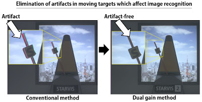
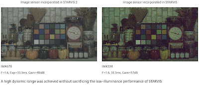
"As the importance of image sensors for security cameras which monitor spaces is growing day by day, the characteristics required of them are also becoming more advanced. Fulfilling all of these requirements, which include low-illuminance performance to allow targets to be discerned even in dark locations, a high dynamic range for face recognition even against a light source such as in entranceways, and performance capable of recording images of moving targets accurately without causing blur or color tints, was a task at a level impossible to accomplish just with improvements to conventional sensors. That is why STARVIS 2 was developed. By redesigning the structure of its image sensor from the ground up, it has successfully implemented characteristics unmatched by any other."


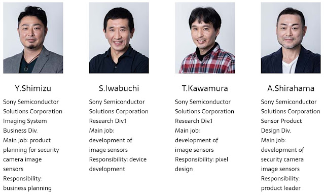
Shimizu:It was triggered by requests from our customers. Although STARVIS had achieved greater low-illuminance sensitivity and improved image quality performance, there were also separate requests to expand its dynamic range so that faces could be accurately recognized even in situations such as entranceways, where the exterior is bright and shooting images against that light source causes faces to become dark and shadowed. Development on STARVIS 2 began to answer these requests.

Shirahama:Normally, we move on to commercialization only after a product’s technology is in place, but since both proceeded simultaneously in this case, we were required to execute development and testing in extremely short cycles. We had no choice but to move forward while resolving each issue one at a time. Because of these conditions, the first prototype was full of problems and was completed in a state that was entirely unacceptable for commercialization.
However, since there was no leeway in the commercialization schedule, delays were not something that could be allowed easily, so the question of how to move the overall project forward while staying aware of its issues was very important. Even when we thought “It’s no use anymore,” we kept an eye on the schedule while resolving each problem, and took one step ahead at a time. And as we did so, our thoughts of “It’s no use anymore” gradually changed more and more into feelings of “Maybe it will work!” Even though the team for this project consisted of members working together for the first time, they possessed the capabilities to solve issues and the flexibility to skillfully move the project forward even under its strict schedule. I began to think “This just may be an incredible team” and working with the team became more and more enjoyable. One of the unique experiences that arose during this project was that as it went forward, the trust we felt toward our team grew and grew.


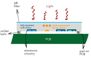
Kawamura:As our development policy, we are constantly making product improvements while maintaining the strengths of the products. This time, in order to address the issue of expanding the dynamic range, there was a need to increase the saturation of the photodiode. Therefore, instead of attaching the photodiode to a conventional silicon surface, we developed a structure which accumulated electric charge in the vertical direction within the silicon.

At the same time, we also introduced new technology for a high dynamic range feature.

We had to proceed with the development of these two new structures that had not yet been established while staying within the schedule for commercialization, so it was a challenge under an extremely tight development period. As Shirahama-san mentioned earlier, there were problems with charge transfer in the initial prototype and it was full of issues, so we were not able to even sufficiently evaluate them.

Iwabuchi:This vertical-structure photodiode had not yet been applied to image sensors, so it was a technology with high risks regarding mass production. Still, we desperately needed a form of breakthrough technology to achieve a wider dynamic range, so since there was a section for prototypes on the development line at Atsugi TEC, we started by trying it out there. We proceeded step-by-step starting from verifying its principles as we marked each development milestone. The commercialization schedule this time had been formulated under the assumption that all parts of technological development would proceed smoothly. As we were faced with successive issues from the very start that did not go as planned, we were continually walking a tightrope to figure out how we could somehow maintain the development schedule.


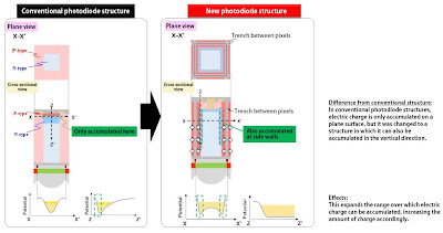
Iwabuchi:To expand the dynamic range, we had to increase the saturation signal while also suppressing noise.
The new vertical structure adopted this time was an innovative structure that could increase the saturation signal amount, but we faced tremendously difficult struggles to optimize the process conditions so that those increased signals could be transmitted reliably.
Regarding the other matter of noise suppression, since both the structure and process were new, we were thoroughly aware of the possibility that the dark characteristics, which were the cause of noise, might become worse.
In order to simultaneously resolve the two issues of increasing the saturation capacity while suppressing noise, we implemented various measures such as reviewing the pixel layout and process conditions, and finally succeeded in developing characteristics to obtain image quality that would fulfill the requests of our customers.

Kawamura:In this project, we made a change to a new pixel structure, but I believe it is still just the beginning. Changing the photodiode to a vertical configuration to make it possible to increase the saturation capacity for greater depth has an enormous amount of hidden potential. I believe it will become essential in the security field to improve image recognition rates, so we intend to further enhance our pixel characteristics such as infrared sensitivity and high dynamic range while also miniaturizing pixels, to make our range of image sensor applications wider than ever before.

Iwabuchi:I believe that Sony’s strengths lie in its ability to carry out advanced development of image sensors with unequaled characteristics that use processes which cannot be copied by competitors, like STARVIS 2. Sony has an atmosphere which encourages new internal challenges, and its engineers in each field are full of motivation to try new things. I hope that we will be able to fully apply the advantages of this environment, to continue to develop revolutionary image sensors distinctive to Sony which are the first of their kind in the world.

Sony Stacked Sensor Inventions

Sony publishes a web page devoted to its notable inventions in stacked image sensors:

The first one is Japanese Patent 5773379 by Taku Umebayashi, Hiroshi Takahashi, and Reijiro Shoji devoted to stacking:


The second notable invention is BSI-optimized photodiode structure in Japanese Patent Number 3759435 by Ryoji Suzuki, Keiji Mabuchi (distinguished inventor at Omnivision now), and Tomonori Mori:


The third and fourth notable inventions are 1975 CCD-era back-illuminated N+NP+N junction type and an N+NP+NP junction type Pinned Photodiode (PPD) (Japanese patent application number 1975-127646, 1975-127647 Yoshiaki Hagiwara) and a PNP junction type PPD with VOD (vertical overflow drain) function (Japanese Patent No. 1215101 Yoshiaki Hagiwara).

Thursday, January 27, 2022

EET-China: For the First Time, Sony Outsources to TSMC Pixel Layer Manufacturing for iPhone 14 Pro Sensor

EET-China and Yahoo-Japan report: "Sony will expand the outsourcing of CMOS image sensor chip manufacturing, of which the pixel layer chip is the first to be manufactured by TSMC.

It is reported that Sony plans to use the 40nm process of TSMC's Nanke Fab 14B plant for its 48-megapixel layer chip, and will upgrade and expand the use of the 28nm mature special process in the future. factory, as well as the joint venture fab JASM in Kumamoto, Japan.

In addition, the logic layer chip at the core of Sony's ISP will also be handed over to TSMC for mass production, using the 22nm process of China's Fab 15A, but the color filter film and microlens process in the latter stage will still be shipped to Sony's own factory in Japan. completed within.

Regarding Sony's change in attitude, the industry believes that this is mainly to meet the demand for the iPhone 14 equipped with a 48-megapixel CMOS image sensor for the first time."

iToF: Comparison of Different Multipath Resolve Methods

IEEE Sensors publishes a video presentation "Multi-Layer ToF: Comparison of Different Multipath Resolve Methods for Indirect 3D Time-of-Flight" by Jonas Gutknecht and Teddy Loeliger from ZHAW School of Engineering, Switzerland.

Abstract: Multipath Interferences (MPI) represent a significant source of error for many 3D indirect time-of-flight (iToF) applications. Several approaches for separating the individual signal paths in case of MPI are described in literature. However, a direct comparison of these approaches is not possible due to the different parameters used in these measurements. In this article, three approaches for MPI separation are compared using the same measurement and simulation data. Besides the known procedures based on the Prony method and the Orthogonal Matching Pursuit (OMP) algorithm, the Particle Swarm Optimization (PSO) algorithm is applied to this problem. For real measurement data, the OMP algorithm has achieved the most reliable results and reduced the mean absolute distance error up to 96% for the tested measurement setups. However, the OMP algorithm limits the minimal distance between two objects with the setup used to approximately 2.7 m. This limitation cannot be significantly reduced even with a considerably higher modulation bandwidth.

Wednesday, January 26, 2022

3D Thermal Imaging Startup Owl Autonomous Imaging Raises $15M in Series-A Round

PRNewswire: Owl Autonomous Imaging (Owl AI), a developer of patented monocular 3D thermal imaging and ranging solutions for automotive active safety systems, today announced $15M in Series A funding.

Owl has developed a patented 3D Thermal Ranging camera, the world's only solid-state camera delivering HD thermal video with high precision ranging for safe autonomous vehicle operation.


Tuesday, January 25, 2022

Facebook Proposes Image Sensing for More Accurate Voice Recognition

Meta (Facebook) publishes a research post "AI that understands speech by looking as well as hearing:"

"People use AI for a wide range of speech recognition and understanding tasks, from enabling smart speakers to developing tools for people who are hard of hearing or who have speech impairments. But oftentimes these speech understanding systems don’t work well in the everyday situations when we need them most: Where multiple people are speaking simultaneously or when there’s lots of background noise. Even sophisticated noise-suppression techniques are often no match for, say, the sound of the ocean during a family beach trip or the background chatter of a bustling street market.

To help us build these more versatile and robust speech recognition tools, we are announcing Audio-Visual Hidden Unit BERT (AV-HuBERT), a state-of-the-art self-supervised framework for understanding speech that learns by both seeing and hearing people speak. It is the first system to jointly model speech and lip movements from unlabeled data — raw video that has not already been transcribed. Using the same amount of transcriptions, AV-HuBERT is 75 percent more accurate than the best audio-visual speech recognition systems (which use both sound and images of the speaker to understand what the person is saying)."

Sony Holds “Sense the Wonder Day”

Sony Semiconductor Solutions Corporation (SSS) held "Sense the Wonder Day," an event to share with a wide range of stakeholders, including employees, the concept behind the company's new corporate slogan, "Sense the Wonder."

At the event, SSS President and CEO Terushi Shimizu introduced SSS as "a company driven by technology and the curiosity of each individual," and explained that SSS's technology "will create the social infrastructure of the future, and will no doubt lead to a 'sensing society' in which image sensors play an active role in all aspects of life." In addition, he said, "The imaging and sensing technologies we create will allow us to uncover new knowledge that makes us question the common sense of the world and discover new richness hidden in our daily lives.