Friday, December 08, 2023

Early announcement: Single Photon Workshop 2024

Single Photon Workshop 2024
EICC Edinburgh 18-22 Nov 2024
www.spw2024.org
 

The 11th Single Photon Workshop (SPW) 2024 will be held 18-24 November 2024, hosted at the Edinburgh International Conference Centre.

SPW is the largest conference in the world dedicated to single-photon generation and detection technology and applications. The biennial international conference brings together a broad range of experts across academia, industry and government bodies with interests in single-photon sources, single-photon detectors, photon entanglement, photonic quantum technologies and their use in scientific and industrial applications. It is an exciting opportunity for those interested in these technologies to learn about the state of the art and to foster continuing partnerships with others seeking to advance the capabilities of such technologies.

In tandem with the scientific programme, SPW 2024 will include a major industry exhibition and networking events.
 
Please register your interest at www.spw2024.org
 
Official registration will open in January 2024.
 
The 2024 workshop is being jointly organized by Heriot-Watt University and University of Glasgow.

Wednesday, December 06, 2023

IISW2023 special issue paper: Small-pitch InGaAs photodiodes

In a new paper titled "Design and Characterization of 5 μm Pitch InGaAs Photodiodes Using In Situ Doping and Shallow Mesa Architecture for SWIR Sensing" Jules Tillement et al. from STMicroelectronics, U. Grenoble and CNRS Grenoble write:

Abstract: This paper presents the complete design, fabrication, and characterization of a shallow-mesa photodiode for short-wave infra-red (SWIR) sensing. We characterized and demonstrated photodiodes collecting 1.55 μm photons with a pixel pitch as small as 3 μm. For a 5 μm pixel pitch photodiode, we measured the external quantum efficiency reaching as high as 54%. With substrate removal and an ideal anti-reflective coating, we estimated the internal quantum efficiency as achieving 77% at 1.55 μm. The best measured dark current density reached 5 nA/cm2 at −0.1 V and at 23 °C. The main contributors responsible for this dark current were investigated through the study of its evolution with temperature. We also highlight the importance of passivation with a perimetric contribution analysis and the correlation between MIS capacitance characterization and dark current performance.

Full paper (open access): https://www.mdpi.com/1424-8220/23/22/9219

Figure 1. Schematic cross section of the photodiode after different processes. (a) Photodiode fabricated by Zn diffusion or Be implantation; (b) photodiode fabrication using shallow mesa technique.

Figure 2. Band diagram of simulated structure at equilibrium with the photogenerated pair schematically represented with their path of collection.


Figure 3. Top zoom of the structure—Impact of the N-InP (a) thickness and (b) doping on the band diagram at equilibrium.

Figure 4. Simulated dark current with TCAD Synopsys tools [28]. (a) Shows evolution of the dark current when the InP SRH lifetime is modulated; (b) evolution of the dark current when the InGaAs SRH lifetime is modulated.

Figure 5. Impact of the doping concentration of the InP barrier on the carrier collection.

Figure 6. Simplified and schematic process flow of the shallow mesa-type process. (a) The full stack; (b) the definition of the pixel by etching the P layer and (c) the encapsulation and fabrication of contacts.

Figure 7. SEM views after the whole process. (a) A cross-section of the top stack where the P layer is etched and (b) a top view of the different configuration of the test structures (single in-array diode is not shown on this SEM view).

Figure 8. Schematic cross section of the structure with its potential sources of the dark current.


Figure 9. Dark current measurement on 15 μm pitch in a matrix like environment. The curve is the median of more than 100 single in-array diodes measured.

Figure 10. Dark current measurement of the ten-by-ten diode bundle. This measurement is from process B.

Figure 11. Evolution of the dark current with temperature at −0.1 V. The solid lines show the theoretical evolution of the current limited by diffusion (light blue line) and by generation recombination (purple line). The temperature measurement is performed on a bundle of ten-by-ten 5 μm pixel pitch diodes.

Figure 12. Perimetric and bulk contribution to the global dark current from measurements performed on diodes with diameter ranging from 10 to 120 μm.

Figure 13. (a) Capacitance measurement on metal–insulator–semiconductor structure. The measurement starts at 0 V then ramps to +40 V then goes to −40 V and ends at +40 V. (b) A cross section of the MIS structure. The MIS is a 300 μm diameter circle.

Figure 14. Dark current performances compared to the hysteresis measured on several different wafers.

Figure 15. Dark current measurement of a ten-by-ten bundle of 5 μm pixel pitch photodiode. The measurements are conducted at 23 °C.

Figure 16. (a) Schematic test structure for QE measurement; (b) the results of the 3D FDTD simulations conducted with Lumerical to estimate the internal QE of the photodiode.


Figure 18. Current noise for a ten-by-ten 5 μm pixel pitch photodiode bundle measured at −0.1 V.

Figure 19. Median current measurement for bundles of one hundred 3 μm pixel pitch photodiodes under dark and SWIR illumination conditions. The dark blue line represents the dark current and the pink line is the photocurrent under 1.55 μm illumination.

Figure 20. Comparison of our work in blue versus the state of the art for the fabrication of InGaAs photodiodes.

Tuesday, December 05, 2023

Sony announces new 5MP SWIR sensor IMX992

Product page: https://www.sony-semicon.com/en/products/is/industry/swir/imx992-993.html

Press release: https://www.sony-semicon.com/en/news/2023/2023112901.html

Sony Semiconductor Solutions to Release SWIR Image Sensor for Industrial Applications with Industry-Leading 5.32 Effective Megapixels Expanding the lineup for delivering high-resolution and low-light performance 


Atsugi, Japan — Sony Semiconductor Solutions Corporation (SSS) today announced the upcoming release of the IMX992 short-wavelength infrared (SWIR) image sensor for industrial equipment, with the industry’s highest pixel count, at 5.32 effective megapixels.

The new sensor uses SSS’s proprietary Cu-Cu connection to achieve the industry’s smallest pixel size of 3.45 μm among SWIR image sensors. It also features an optimized pixel structure for efficiently capturing light, enabling high-definition imaging across a broad spectrum ranging from the visible to invisible short-wavelength infrared regions (wavelength: 0.4 to 1.7 μm). Furthermore, new shooting modes deliver high-quality images with significantly reduced noise in dark environments compared to conventional products.

In addition to this product, SSS will also release the IMX993 with a pixel size of 3.45 μm and an effective pixel count of 3.21 megapixels to further expand its SWIR image sensor lineup. These new SWIR image sensors with high pixel counts and high sensitivity will help contribute to the evolution of various industrial equipment.

In the industrial equipment domain in recent years, there has been increasing demand for improving productivity and preventing defective products from leaving the plant. In this context, the capacity to sense not only visible light but also light in the invisible band is in demand. SSS’s SWIR image sensors, which are capable of seamless wide spectrum imaging in the visible to invisible short-wavelength infrared range using a single camera, are already being used in various processes such as semiconductor wafer bonding and defect inspection, as well as ingredient and contaminant inspections in food production.

The new sensors enable imaging with higher resolution using pixel miniaturization, while enhancing imaging performance in low-light environments to provide higher quality imaging in inspection and monitoring applications conducted in darker conditions. By making the most of the characteristics of short-wavelength infrared light, whose light reflection and absorption properties are different from those of visible light, these products help to further expand applications in such areas as inspection, recognition and measurement, thereby contributing to improved industrial productivity.

Main Features
* High pixel count made possible by the industry’s smallest pixels at 3.45 μm, delivering high-resolution imaging

A Cu-Cu connection is used between the indium-gallium arsenide (InGaAs) layer that forms the photodiode of the light receiving unit and the silicon (Si) layer that forms the readout circuit. This design allows for a smaller pixel pitch, resulting in the industry’s smallest pixel size of 3.45 μm. This, in turn, helps achieve a compact form factor that still delivers the industry’s highest pixel count of approximately 5.32 effective megapixels on the IMX992, and approximately 3.21 effective megapixels on the IMX993. The higher pixel count enables detection of tiny objects or imaging across a wide range, contributing to significantly improved recognition and measurement precision in various inspections using short-wavelength infrared light.


 Comparison of SWIR images with different resolutions: Lighting wavelength 1550 nm
(Left: Other SSS product, 1.34 effective megapixels; Right: IMX992)

* Low-noise imaging even in dark locations possible by switching the shooting mode

Inclusion of new shooting modes enables low-noise imaging without being affected by environmental brightness. In dark environments with limited light, High Conversion Gain (HCG) mode directly amplifies the signal with minimal noise after being converted to an electrical signal from light, thereby relatively reducing the amount of noise downstream. Doing so minimizes the impact of noise in dark locations, leading to greater recognition precision. On the other hand, in bright environments with plenty of light, Low Conversion Gain (LCG) mode enables imaging prioritizing the dynamic range.
Furthermore, enabling Dual Read Rolling Shutter (DRRS) outputs images from the sensor in two distinct types. These images are then composited on the camera to acquire an image with significantly reduced noise.

Image quality and noise comparison in dark location: Lighting wavelength 1450 nm
(Left: Other SSS product, 1.34 effective megapixels; Center: IMX992, HCG mode selected; Right: IMX992, HCG mode selected, DRRS enabled)


* Optimized pixel structure for high-sensitivity imaging across a wide range

SSS’s SWIR image sensors employ a thinner indium-phosphorous (InP) layer on top, which would otherwise inevitably absorb visible light, thereby allowing visible light to reach the indium-gallium arsenide (InGaAs) layer underneath, delivering high quantum efficiency even in the visible wavelength. The new products deliver even higher quantum efficiency by optimizing the pixel structure, enabling more uniform sensitivity characteristics across a wide wavelength band from 0.4 to 1.7 μm. Minimizing the image quality differences between wavelengths makes it possible to use the image sensor in a variety of industrial applications and contributes to improved reliability in inspection, recognition, and measurement applications.


Product Overview


Monday, December 04, 2023

Prof. Edoardo Charbon's Talk on IR SPADs for LiDAR & Quantum Imaging


SWIR/NIR SPAD Image Sensors for LIDAR and Quantum Imaging Applications, by Prof. Charbon

In this talk, prof. Charbon will review the evolution of solid-state photon counting sensors from avalanche photodiodes (APDs) to silicon photomultipliers (SiPMs) to single-photon avalanche diodes (SPADs). The impact of these sensors on LiDAR has been remarkable, however, more innovations are to come with the continuous advance of integrated SPADs and the introduction of powerful computational imaging techniques directly coupled to SPADs/SiPMs. New technologies, such as 3D-stacking in combination with Ge and InP/InGaAs SPAD sensors, are accelerating the adoption of SWIR/NIR image sensors, while enabling new sensing functionalities. Prof. Charbon will conclude the talk with a technological perspective on how all these technologies could come together in low-cost, computational-intensive image sensors, for affordable, yet powerful quantum imaging

Edoardo Charbon (SM’00 F’17) received the Diploma from ETH Zurich, the M.S. from the University of California at San Diego, and the Ph.D. from the University of California at Berkeley in 1988, 1991, and 1995, respectively, all in electrical engineering and EECS. He has consulted with numerous organizations, including Bosch, X-Fab, Texas Instruments, Maxim, Sony, Agilent, and the Carlyle Group. He was with Cadence Design Systems from 1995 to 2000, where he was the Architect of the company's initiative on information hiding for intellectual property protection. In 2000, he joined Canesta Inc., as the Chief Architect, where he led the development of wireless 3-D CMOS image sensors.
Since 2002 he has been a member of the faculty of EPFL, where is a full professor. From 2008 to 2016 he was with Delft University of Technology’s as Chair of VLSI design. Dr. Charbon has been the driving force behind the creation of deep-submicron CMOS SPAD technology, which is mass-produced since 2015 and is present in telemeters, proximity sensors, and medical diagnostics tools. His interests span from 3-D vision, LiDAR, FLIM, FCS, NIROT to super-resolution microscopy, time-resolved Raman spectroscopy, and cryo-CMOS circuits and systems for quantum computing. He has authored or co-authored over 400 papers and two books, and he holds 24 patents. Dr. Charbon is the recipient of the 2023 IISS Pioneering Achievement Award, he is a distinguished visiting scholar of the W. M. Keck Institute for Space at Caltech, a fellow of the Kavli Institute of Nanoscience Delft, a distinguished lecturer of the IEEE Photonics Society, and a fellow of the IEEE.

Sunday, December 03, 2023

Job Postings - Week of 3 Dec 2023


Johnson & Johnson

Principal Electrical Engineer – Vision

Santa Clara, California, USA

Cincinnati, Ohio, USA

Link

Shenzhen Institute of Advanced Technology

Faculty positions in Research Center for Intelligent Biomedical Materials and Devices (IBMD)

Shenzhen, Guangdong, China

Link

Andor Technology

Physicist

Belfast, Northern Ireland, UK

Link

Bruker

Application Scientist Magnetic Particle Imaging

Ettlingen, Germany

Link

Raytheon

EO - Senior Principal Optical Subsystems Engineer

Tucson, Arizona, USA

Link

Telops

R&D Project Manager

Quebec City, Quebec, Canada

Link

CERN

R&D on CMOS detectors for the new experiments at the Future Circular Collider

Geneva, Switzerland

Link

University of Sussex

PhD studentship on novel opaque scintillator detector R&D

Brighton, UK

Link


Friday, December 01, 2023

Prophesee event sensor in 2023 VLSI symposium

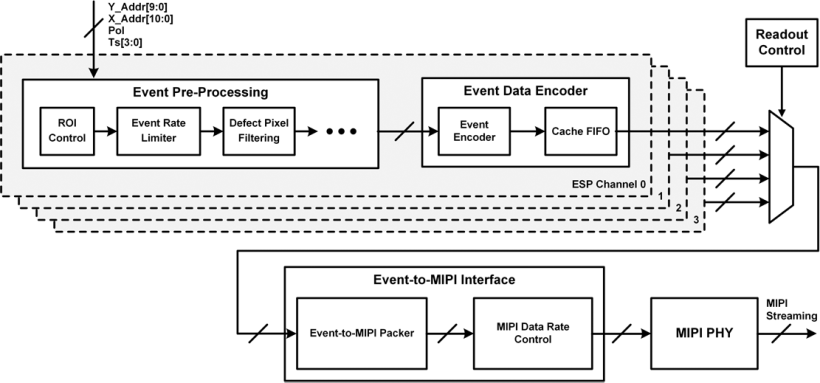
Schon et al from Prophesee published a paper titled "A 320 x 320 1/5" BSI-CMOS stacked event sensor for low-power vision applications" in the 2023 VLSI symposium. This paper presents some technical details about their recently announced GenX320 sensor.

Abstract
Event vision sensors acquire sparse data, making them suited for edge vision applications. However, unconventional data format, nonconstant data rates and non-standard interfaces restrain wide adoption. A 320x320 6.3μm pixel BSI stacked
event sensor, specifically designed for embedded vision, features multiple data pre-processing, filtering and formatting functions, variable MIPI and CPI interfaces and a hierarchy of power modes, facilitating operability in power-sensitive vision
applications.


Thursday, November 30, 2023

ISSCC 2024 Advanced Program Now Available

ISSCC will be held Feb 18-22, 2024 in San Francisco, CA.

Link to advanced program: https://submissions.mirasmart.com/ISSCC2024/PDF/ISSCC2024AdvanceProgram.pdf

There are several papers of interest in Session 6 on Imagers and Ultrasound. 

6.1 12Mb/s 4×4 Ultrasound MIMO Relay with Wireless Power and Communication for Neural Interfaces
E. So, A. Arbabian (Stanford University, Stanford, CA)

6.2 An Ultrasound-Powering TX with a Global Charge-Redistribution Adiabatic Drive Achieving 69% Power Reduction and 53° Maximum Beam Steering Angle for Implantable Applications
M. Gourdouparis1,2, C. Shi1 , Y. He1 , S. Stanzione1 , R. Ukropec3 , P. Gijsenbergh3 , V. Rochus3 , N. Van Helleputte3 , W. Serdijn2 , Y-H. Liu1,2
 1 imec, Eindhoven, The Netherlands
 2 Delft University of Technology, Delft, The Netherlands
 3 imec, Leuven, Belgium

6.3 Imager with In-Sensor Event Detection and Morphological Transformations with 2.9pJ/pixel×frame Object Segmentation FOM for Always-On Surveillance in 40nm
 J. Vohra, A. Gupta, M. Alioto, National University of Singapore, Singapore, Singapore

6.4 A Resonant High-Voltage Pulser for Battery-Powered Ultrasound Devices
 I. Bellouki1 , N. Rozsa1 , Z-Y. Chang1 , Z. Chen1 , M. Tan1,2, M. Pertijs1
 1 Delft University of Technology, Delft, The Netherlands
 2 SonoSilicon, Hangzhou, China

6.5 A 0.5°-Resolution Hybrid Dual-Band Ultrasound Imaging SoC for UAV Applications
 J. Guo1 , J. Feng1 , S. Chen1 , L. Wu1 , C-W. Tsai1,2, Y. Huang1 , B. Lin1 , J. Yoo1,2
 1 National University of Singapore, Singapore, Singapore
 2 The N.1 Institute for Health, Singapore, Singapore

6.6 A 10,000 Inference/s Vision Chip with SPAD Imaging and Reconfigurable Intelligent Spike-Based Vision Processor
 X. Yang*1 , F. Lei*1 , N. Tian*1 , C. Shi2 , Z. Wang1 , S. Yu1 , R. Dou1 , P. Feng1 , N. Qi1 , J. Liu1 , N. Wu1 , L. Liu1
 1 Chinese Academy of Sciences, Beijing, China 2 Chongqing University, Chongqing, China
 *Equally Credited Authors (ECAs)

6.7 A 160×120 Flash LiDAR Sensor with Fully Analog-Assisted In-Pixel Histogramming TDC Based on Self-Referenced SAR ADC
 S-H. Han1 , S. Park1 , J-H. Chun2,3, J. Choi2,3, S-J. Kim1
 1 Ulsan National Institute of Science and Technology, Ulsan, Korea
 2 Sungkyunkwan University, Suwon, Korea
 3 SolidVue, Seongnam, Korea

6.8 A 256×192-Pixel 30fps Automotive Direct Time-of-Flight LiDAR Using 8× Current-Integrating-Based TIA, Hybrid Pulse Position/Width Converter, and Intensity/CNN-Guided 3D Inpainting
 C. Zou1 , Y. Ou1 , Y. Zhu1 , R. P. Martins1,2, C-H. Chan1 , M. Zhang1
 1 University of Macau, Macau, China
 2 Instituto Superior Tecnico/University of Lisboa, Lisbon, Portugal

6.9 A 0.35V 0.367TOPS/W Image Sensor with 3-Layer Optical-Electronic Hybrid Convolutional Neural Network
 X. Wang*, Z. Huang*, T. Liu, W. Shi, H. Chen, M. Zhang
 Tsinghua University, Beijing, China
 *Equally Credited Authors (ECAs)

6.10 A 1/1.56-inch 50Mpixel CMOS Image Sensor with 0.5μm pitch Quad Photodiode Separated by Front Deep Trench Isolation
 D. Kim, K. Cho, H-C. Ji, M. Kim, J. Kim, T. Kim, S. Seo, D. Im, Y-N. Lee, J. Choi, S. Yoon, I. Noh, J. Kim, K. J. Lee, H. Jung, J. Shin, H. Hur, K. E. Chang, I. Cho, K. Woo, B. S. Moon, J. Kim, Y. Ahn, D. Sim, S. Park, W. Lee, K. Kim, C. K. Chang, H. Yoon, J. Kim, S-I. Kim, H. Kim, C-R. Moon, J. Song
 Samsung Semiconductor, Hwaseong, Korea

6.11 A 320x240 CMOS LiDAR Sensor with 6-Transistor nMOS-Only SPAD Analog Front-End and Area-Efficient Priority Histogram Memory
 M. Kim*1 , H. Seo*1,2, S. Kim1 , J-H. Chun1,2, S-J. Kim3 , J. Choi*1,2
 1 Sungkyunkwan University, Suwon, Korea
 2 SolidVue, Seongnam, Korea
 3 Ulsan National Institute of Science and Technology, Ulsan, Korea
 *Equally Credited Authors (ECAs)
 

Imaging papers in other sessions: 

17.3 A Fully Wireless, Miniaturized, Multicolor Fluorescence Image Sensor Implant for Real-Time Monitoring in Cancer Therapy
 R. Rabbani*1 , M. Roschelle*1 , S. Gweon1 , R. Kumar1 , A. Vercruysse1 , N. W. Cho2 , M. H. Spitzer2 , A. M. Niknejad1 , V. M. Stojanovic1 , M. Anwar1,2
 1 University of California, Berkeley, CA
 2 University of California, San Francisco, CA
 *Equally Credited Authors (ECAs)

33.10 A 2.7ps-ToF-Resolution and 12.5mW Frequency-Domain NIRS Readout IC with Dynamic Light Sensing Frontend and Cross-Coupling-Free Inter-Stabilized Data Converter
 Z. Ma1 , Y. Lin1 , C. Chen1 , X. Qi1 , Y. Li1 , K-T. Tang2 , F. Wang3 , T. Zhang4 , G. Wang1 , J. Zhao1
 1 Shanghai Jiao Tong University, Shanghai, China
 2 National Tsing Hua University, Hsinchu, Taiwan
 3 Shanghai United Imaging Microelectronics Technology, Shanghai, China
 4 Shanghai Mental Health Center, Shanghai, China

Wednesday, November 29, 2023

IISW2023 special issue paper on well capacity of pinned photodiodes

Miyauchi et al from Brillnics and  Tohoku University published a paper titled "Analysis of Light Intensity and Charge Holding Time Dependence of Pinned Photodiode Full Well Capacity" in the IISW 2023 special issue of the journal Sensors.

Abstract
In this paper, the light intensity and charge holding time dependence of pinned photodiode (PD) full well capacity (FWC) are studied for our pixel structure with a buried overflow path under the transfer gate. The formulae for PDFWC derived from a simple analytical model show that the relation between light intensity and PDFWC is logarithmic because PDFWC is determined by the balance between the photo-generated current and overflow current under the bright condition. Furthermore, with using pulsed light before a charge holding operation in PD, the accumulated charges in PD decrease with the holding time due to the overflow current, and finally, it reaches equilibrium PDFWC. The analytical model has been successfully validated by the technology computer-aided design (TCAD) device simulation and actual device measurement.

Open access: https://doi.org/10.3390/s23218847

Figure 1. Measured dynamic behaviors of PPD.

Figure 2. Pixel schematic and pulse timing for characterization.

Figure 3. PD cross-section and potential of the buried overflow path.

Figure 4. Potential and charge distribution changes from PD reset to PD saturation.

Figure 5. Simple PD model for theoretical analysis.
Figure 6. A simple model of dynamic behavior from PD reset to PD saturation under static light condition.

Figure 7. Potential and charge distribution changes from PD saturation to equilibrium PDFWC.

Figure 8. A simple model of PD charge reduction during charge holding operation with pulse light.
Figure 9. Chip micrograph and specifications of our developed stacked 3Q-DPS [7,8,9].


Figure 10. Relation between ∆Vb and Iof with static TCAD simulation.
Figure 12. PDFWC under various light intensity conditions.
Figure 13. PDFWC with long charge holding times.
Figure 14. TCAD simulation results of equilibrium PDFWC potential.


Monday, November 27, 2023

Sony announces full-frame global shutter camera

Link: https://www.sony.com/lr/electronics/interchangeable-lens-cameras/ilce-9m3

Sony recently announced a full-frame global shutter camera which was featured in several press articles below:


PetaPixel https://petapixel.com/2023/11/07/sony-announces-a9-iii-worlds-first-global-sensor-full-frame-camera/

DPReview https://www.dpreview.com/news/7271416294/sony-announces-a9-iii-world-s-first-full-frame-global-shutter-camera

The Verge https://www.theverge.com/2023/11/7/23950504/sony-a9-iii-mirrorless-camera-global-shutter-price-release


From Sony's official webpage:

[This camera uses the] Newly developed full-frame stacked 24.6 MP Exmor RS™ image sensor with global shutter [...] a stacked CMOS architecture and integral memory [...] advanced A/D conversion enable high-speed processing to proceed with minimal delay. [AI features are implemented using the] BIONZ XR™ processing engine. With up to eight times more processing power than previous versions, the BIONZ XR image processing engine minimises processing latency [...] It's able to process the high volume of data generated by the newly developed Exmor RS image sensor in real-time, even while shooting continuous bursts at up to 120 fps, and it can capture high-quality 14-bit RAW images in all still shooting modes. [...] [The] α9 III can use subject form data to accurately recognise movement. Human pose estimation technology recognises not just eyes but also body and head position with high precision. 


Sunday, November 26, 2023

Job Postings - Week of 26 Nov 2023

Apple

Hardware Sensing Systems Engineer

Cupertino, California, USA

Link

Friedrich-Schiller-Universität Jena

2 PhD scholarships in Optics & Photonics

Jena, Germany

Link

Rice University

Open Rank Faculty Position in Advanced Materials

Houston, Texas, USA

Link

Caeleste

Image Sensor Architect

Mechelen, Belgium

Link

BAE Systems (Secret Clearance)

FAST Labs - Multi-Function Sensor Systems Chief Scientist (US only)

Merrimack, New Hampshire,  USA

Link

LYNRED

HgCdTe Epitaxy on Quaternary Substrates (6-month contract)

Veurey-Voroize, France

Link

Princeton Infrared Technologies

Camera Development Manager/Engineer

Monmouth Junction, New Jersey, USA

Link

Rutherford Appleton Laboratory

Senior Project Manager, Imaging Systems Division

Didcot, Oxfordshire, England

Link

Excelitas

Wafer Fab Engineering Mgr

Billerica, Massachusetts, USA

Link