Thursday, February 29, 2024

STMicroelectronics announces new ToF Sensors

VD55H1 Low-Noise Low-Power iToF Sensor
-- New design feat, packing 672 x 804 sensing pixels in a tiny chip size and can map a three-dimensional surface in great detail by measuring distance to over half a million points.
-- Lanxin Technology will use the VD55H1 for intelligent obstacle avoidance and high-precision docking in mobile robots; MRDVS will enhance its 3D cameras adding high-accuracy depth-sensing. 


VL53L9 dToF 3D Lidar Module
-- New high-resolution sensor with 5cm – 9m ranging distance ensures accurate depth measurements for camera assistance, hand tracking, and gesture recognition.
-- VR systems use the VL53L9 to depict depth more accurately within 2D and 3D imaging, improving mapping for immersive gaming and other applications like 3D avatars.

The two new products announced will enhance safer mobile robots in industrial environments​ and smart homes as well as enable advanced VR applications.


The VL53L9CA is a state of the art, dToF 3D lidar (light detection and ranging) module with market leading resolution of up to 2.3k zones and accurate ranging from 5cm to 10m.


Full press release:

STMicroelectronics expands into 3D depth sensing with latest time-of-flight sensors

STMicroelectronics (NYSE: STM), a global semiconductor leader serving customers across the spectrum of electronics applications, announced an all-in-one, direct Time-of-Flight (dToF) 3D LiDAR (Light Detection And Ranging) module with market-leading 2.3k resolution, and revealed an early design win for the world’s smallest 500k-pixel indirect Time-of-Flight (iToF) sensor.
 
“ToF sensors, which can accurately measure the distance to objects in a scene, are driving exciting new capabilities in smart devices, home appliances, and industrial automation. We have already delivered two billion sensors into the market and continue to extend our unique portfolio, which covers all types from the simplest single-zone devices up to our latest high-resolution 3D indirect and direct ToF sensors,” said Alexandre Balmefrezol, General Manager, Imaging Sub-Group at STMicroelectronics. “Our vertically integrated supply chain, covering everything from pixel and metasurface lens technology and design to fabrication, with geographically diversified in-house high-volume module assembly plants, lets us deliver extremely innovative, highly integrated, and high-performing sensors.”
 
The VL53L9, announced today, is a new direct ToF 3D LiDAR device with a resolution of up to 2.3k zones. Integrating a dual scan flood illumination, unique in the market, the LiDAR can detect small objects and edges and captures both 2D infrared (IR) images and 3D depth map information. It comes as a ready-to-use low power module with its on-chip dToF processing, requiring no extra external components or calibration. Additionally, the device delivers state-of-the-art ranging performance from 5cm to 10 meters.
 
VL53L9’s suite of features elevates camera-assist performance, supporting macro up to telephoto photography. It enables features such as laser autofocus, bokeh, and cinematic effects for still and video at 60fps (frame per second). Virtual reality (VR) systems can leverage accurate depth and 2D images to enhance spatial mapping for more immersive gaming and other VR experiences like virtual visits or 3D avatars. In addition, the sensor’s ability to detect the edges of small objects at short and ultra-long ranges makes it suitable for applications such as virtual reality or SLAM (simultaneous localization and mapping).
 
ST is also announcing news of its VD55H1 ToF sensor, including the start of volume production and an early design win with Lanxin Technology, a China-based company focusing on mobile-robot deep-vision systems. MRDVS, a subsidiary company, has chosen the VD55H1 to add high-accuracy depth-sensing to its 3D cameras. The high-performance, ultra-compact cameras with ST’s sensor inside combine the power of 3D vision and edge AI, delivering intelligent obstacle avoidance and high-precision docking in mobile robots.

In addition to machine vision, the VD55H1 is ideal for 3D webcams and PC applications, 3D reconstruction for VR headsets, people counting and activity detection in smart homes and buildings. It packs 672 x 804 sensing pixels in a tiny chip size and can accurately map a three-dimensional surface by measuring distance to over half a million points. ST’s stacked-wafer manufacturing process with backside illumination enables unparalleled resolution with smaller die size and lower power consumption than alternative iToF sensors in the market. These characteristics give the sensors their excellent credentials in 3D content creation for webcams and VR applications including virtual avatars, hand modeling and gaming.

First samples of the VL53L9 are already available for lead customers and mass production is scheduled for early 2025. The VD55H1 is in full production now.

Pricing information and sample requests are available at local ST sales offices. ST will showcase a range of ToF sensors including the VL53L9 and explain more about its technologies at Mobile World Congress 2024, in Barcelona, February 26-29, at booth 7A61.
 

Wednesday, February 28, 2024

Five Jobs from Omnivision in Norway and Belgium

 Omnivision has sent us the following list of openings in their CMOS sensor development teams -

In Oslo, Norway:

Analog Characterization Engineer   Link

Functional Safety Verification Engineer   Link

Sr. Digital Design Engineer   Link

Staff Digital Design Engineer   Link

In Mechelen, Belgium:

Staff Characterization Engineer   Link

Jobs Submitted by Employers

Sony Depthsensing Solutions (23 Apr 2024)  Link
 
STMicroelectronics (6 Apr 2024)   Link
 
KU Leuven (4 Apr 2024)    Link

Sony EUTDC (31 Mar 2024)   Link

Euresys (21 Mar 2024)   Link

onsemi (11 Feb 2024)   Link 

Sony (7 Feb 2024)    Link

Qurv (3 Feb 2024)   Link 

Photonis - (31 Jan 2024)   Link 

Sony Semiconductor Solutions - America (25 Jan 2024)   Link

CEA Leti (23 Jan 2024)   Link 

ISAE SUPAERO (23 Jan 2024)   Link  

Transformative Optics (20 Jan 2024)   Link

Teledyne (13 Dec 2023)   Link

Sunday, February 25, 2024

Job Postings - Week of 25 February 2024

Sony UK Technology Centre

Industrial Engineer

Penceod, Wales, UK

Link

Apple

Image Quality Analyst

San Diego, California, USA

Link

Jenoptik

Imaging Engineer

Camberley, England, UK

Link

NASA

Postdoc - Materials and Process Development for Ultraviolet Detector Technologies (apply by 1 Mar 2024)

Pasadena, California, USA

Link

ASML

Research Group Lead Sensor Modelling and Computational Imaging

Veldhoven, Netherlands

Link

Brookhaven National Laboratory

Deputy Director-Instrumentation Division

Upton, New York, USA

Link

Axon

Principal Systems Engineer (Remote)

Scottsdale, Arizona, USA

Link

Rochester Institute of Technology

Tenure Track Faculty – Center for Imaging Science

Rochester, New York, USA

Link

Science and Technology Facilities Council – Rutherford Appleton

Detector Scientist Industrial Placement

Didcot, Oxfordshire, England, UK

Link


Saturday, February 24, 2024

Conference List - August 2024

International Symposium on Sensor Science - 1-4 Aug 2024 - Singapore - Website

Quantum Structure Infrared Photodetector (QSIP)  International Conference - 12-16 Aug 2024 - Santa Barbara, California, USA - Website

SPIE Optics & Photonics - 18-22 Aug 2024 - San Diego, California, USA - Website

International Conference on Sensors and Sensing Technology - 29-31 August 2024 - Valencia, Spain - Website

If you know about additional local conferences, please add them as comments.

Return to Conference List index


Friday, February 23, 2024

Teledyne acquires Adimec

From Metrology News: https://metrology.news/teledyne-to-acquire-high-performance-camera-specialist-adimec/

Teledyne to Acquire High-Performance Camera Specialist Adimec

Teledyne Technologies has announced that it has entered into an agreement to acquire Adimec Holding B.V. and its subsidiaries (Adimec). Adimec, founded in 1992 and headquartered in Eindhoven, Netherlands, develops customized high-performance industrial and scientific cameras for applications where image quality is of paramount importance.

​“Adimec possesses uniquely complementary technology, products and customers in the shared strategic focus areas of healthcare, global defense, and semiconductor and electronics inspection,” said Edwin Roks, Chief Executive Officer of Teledyne. “For decades and from our own X-ray imaging business headquartered in Eindhoven, I have watched Adimec grow to become a leader in niche applications requiring truly accurate images for precise decision making in time-critical processes.”

Joost van Kuijk, Adimec’s Chief Executive Officer, commented, “It is with great pleasure that we are able to announce publicly that Adimec will become part of Teledyne. Adimec’s success has always been built on ensuring imaging excellence in demanding applications through an unwavering focus on individual customer requirements by our expert engineers and designers.”

Adimec co- Chief Executive Officer, Alex de Boer added, “As a leader in advanced imaging technologies for industrial and scientific markets, Teledyne is the perfect company to build further on the strong foundation the founders and management have established over the past three decades. The entire Adimec team is looking forward to contributing to an exciting future with Teledyne while extending technical boundaries to support our customers with cameras – perfectly optimized to their application needs.”

Wednesday, February 21, 2024

Computational Imaging Photon by Photon


Arizona Optical Sciences Colloquium: Andreas Velten, "Computational Imaging Photon by Photon"

Abstract
Our cameras usually measure light as an analog flux that varies as a function of space and time. This approximation ignores the quantum nature of light which is actually made of discrete photons each of which is collected at a sensor pixel at an instant in time. Single photon cameras have pixels that can detect photons and the timing of their arrival resulting in cameras with unprecedented capabilities. Concepts like motion blur, exposure time, and dynamic range that are essential to conventional cameras do not really apply to single photon sensors. In this presentation I will cover computational imaging capabilities enabled by single photon cameras and their applications.

The extreme time resolution of single photon cameras enables time of flight measurements we use for Non-Line-of-Sight (NLOS) Imaging. NLOS systems reconstruct images of scene using indirect light from reflections off a diffuse relay surface. After illuminating the relay surface with short pulses, the returning light is detected with high time resolution single photon cameras. We thereby capture video of the light propagation in the visible scene and reconstruct images of hidden parts of the scene.

Over the past decade NLOS imaging has seen rapid progress and we can now capture and reconstruct hidden scenes in real time and with high image quality. In this presentation I will give an overview over the imaging using single photon avalanche diodes, reconstruction methods, and applications driving NLOS imaging and provide an outlook for future development.

Bio
Andreas Velten is Associate Professor at the Department of Biostatistics and Medical Informatics and the Department of Electrical and Computer Engineering at the University of Wisconsin-Madison and directs the Computational Optics Group. He obtained his PhD with Prof. Jean-Claude Diels in Physics at the University of New Mexico in Albuquerque and was a postdoctoral associate of the Camera Culture Group at the MIT Media Lab. He has included in the MIT TR35 list of the world's top innovators under the age of 35 and is a senior member of NAI, OSA, and SPIE as well as a member of Sigma Xi. He is co-Founder of Onlume, a company that develops surgical imaging systems, and Ubicept, a company developing single photon imaging solutions.

Monday, February 19, 2024

SolidVue develops solid-state LiDAR chip

From PR Newswire: https://www.prnewswire.com/news-releases/solidvue-koreas-exclusive-developer-of-lidar-sensor-chips-showcasing-world-class-technological-capabilities-302018487.html

SolidVue, Korea's Exclusive Developer of LiDAR Sensor Chips Showcasing World-Class Technological Capabilities 

SEOUL, South Korea, Dec. 19, 2023 /PRNewswire/ -- SolidVue Inc., Korea's exclusive enterprise specialized in CMOS LiDAR (Light Detection and Ranging) sensor IC development, once again proved its global technological prowess by announcing its achievement of two LiDAR-related papers being accepted at the upcoming 'ISSCC (International Solid-State Circuits Conference) 2024'.

Established in 2020, SolidVue focuses on designing SoCs (System-on-Chip) for LiDAR sensors that comprehensively assesses the shapes and distances of surrounding objects. This is a pivotal technology assured to see significant growth in industries such as but not limited to autonomous vehicles and smart cities.

Jaehyuk Choi, the CEO of SolidVue, disclosed the company's development of Solid-State LiDAR sensor chips, aiming to replace all components of traditional mechanical LiDAR with semiconductors. This innovation is expected to reduce volume by up to one-tenth and costs by around one-hundredth compared to the aforementioned mechanical LiDAR.

Utilizing its proprietary CMOS SPAD (Single Photon Avalanche Diode) technology, SolidVue's LiDAR sensor chips flawlessly detect even minute particles of light, enhancing measurement precision. The company focuses on all LiDAR detection ranges (short, medium, long), notably making advancements in the medium-to-long distance sector suited for autonomous vehicles and robotics. By the third quarter of this year, they meticulously developed an Engineering Sample (ES) of a Solid-State LiDAR sensor chip capable of measuring up to 150 meters, and are aiming for mass production by the end of 2024.
Choi emphasized SolidVue's independent development of various core technologies such as SPAD devices, LiDAR sensor architectures, and integrated image signal processors, while also highlighting the advantage of SolidVue's single-chip design in cost and size reduction compared to the multi-chip setup of traditional mechanical LiDAR sensors.

SolidVue's technological prowess has been repeatedly acknowledged at the ISSCC, marking a remarkable achievement for a Korean fabless company. At the forthcoming ISSCC 2024, SolidVue is set to showcase its groundbreaking advancements, including a 50-meter mid-range Solid-State LiDAR sensor that features a resolution of 320x240 pixels and optimized memory efficiency. Additionally, a 10-meter short-range Flash LiDAR will be presented, characterized by its 160x120 pixel resolution and an ultra-low power consumption of 3-uW per pixel. These significant innovations are the result of collaborative efforts between SolidVue, Sungkyunkwan University, and UNIST.

Ahead of full product commercialization, SolidVue's focal point is securing domestic and international clients as well as attracting investments. In January, they plan to make their debut at the 'CES 2024', the world's largest electronics exhibition, by showcasing their 150-m LiDAR sensor chip ES products with the aim of initiating discussions and collaborations with leading global LiDAR suppliers.

Since its establishment, SolidVue has secured a cumulative $6 million in investments. Key Korean VCs such as KDB Bank, Smilegate Investment, Quantum Ventures Korea, Quad Ventures, among others, have participated as financial investors. Additionally, Furonteer, a company specializing in automated equipment for automotive camera modules, joined as SolidVue's first strategic investor.

CEO Choi stated, "Aligning with the projected surge in LiDAR demand post-2026, we are laying the groundwork for product commercialization." He added, "We are heavily engaged in joint research and development with major Korean corporations, discussing numerous LiDAR module supply deals, and exploring collaborations with global companies for overseas market penetration."

SolidVue’s LiDAR sensor chip and demonstration images (Photo=SolidVue)


Sunday, February 18, 2024

Job Postings - Week of 18 February 2024

Pacific Biosciences

Staff CMOS Sensor Test Engineer

Menlo Park, California, USA

Link

Vilnius University

PostDoc in Experimental HEP

Vilnius, Lithuania

Link

Precision Optics Corporation

Electrical Engineer

Windham, Maine, USA

Link

CEDES

(Senior) Design Engineer in Product Development

Singapore

Link

Karl Storz

Image Processing Engineer V

Goleta, California, USA

Link

Karl Storz

Development Engineer - Image Processing

Tuttlingen, Germany

Link

University of Warwick

PhD Studentship: Towards Silicon Photonics Based Gas Sensors

Coventry, UK

Link

Leidos

Optical Test Engineer

Dayton, Ohio, USA

Link

Teledyne e2v Semiconductors

MBE Growth Production Engineer

Camarillo, California, USA

Link

Saturday, February 17, 2024

Conference List - July 2024

The 9th International Smart Sensor Technology Exhibition - 3-5 Jul 2024 - Seoul, Korea (South) - Website

17th International Conference on Scintillating Materials and their Applications - 8-12 Jul 2024 - Milan, Italy - Website

Optica Sensing and Imaging Congresses - 15-19 Jul 2024 - Toulouse, France  - Website

International Conference on Imaging, Signal Processing and Communications - 19-21 Jul 2024 - Fukuoka, Japan - Website

American Association of Physicists in Medicine Annual Meeting - 21-25 Jul 2024 - Los Angeles, California, USA - Website

If you know about additional local conferences, please add them as comments.

Return to Conference List index

Friday, February 16, 2024

Semiconductor Engineering article about noise in CMOS image sensors

Semiconductor Engineering published an article on dealing with noise in CMOS image sensors: https://semiengineering.com/dealing-with-noise-in-image-sensors/

Dealing With Noise In Image Sensors

The expanding use and importance of image sensors in safety-critical applications such as automotive and medical devices has transformed noise from an annoyance into a life-threatening problem that requires a real-time solution.

In consumer cameras, noise typically results in grainy images, often associated with poor lighting, the speed at which an image is captured, or a faulty sensor. Typically, that image can be cleaned up afterward, such as reducing glare in a selfie. But in cars, glare in an ADAS image system can affect how quickly the brakes are applied. And in vehicles or medical devices, systems are so complex that external effects can affect images, including heat, electromagnetic interference, and vibration. This can be particularly problematic in AI-enabled computer vision systems where massive amounts of data need to be processed at extremely high speeds. And any of this can be affected by aging circuits, due to dielectric breakdown or changes in signal paths due to electromigration.

Thresholds for noise tolerance vary by application. “A simple motion-activated security camera or animal-motion detection system at a zoo can tolerate much more noise and operate at much lower resolution than a CT scanner or MRI system used in life-saving medical contexts,” said Brad Jolly, senior applications engineer at Keysight. “[Noise] can mean anything that produces errors in a component or system that acquires any form of image, including visible light, thermal, X-ray, radio frequency (RF), and microwave.”

Tolerance is also determined by human perception, explained Andreas Suess, senior manager for novel image sensor systems in OmniVision’s Office of the CTO. “Humans perceive an image as pleasing with a signal-to-noise ratio (SNR) of >20dB, ideally >40dB. But objects can often be seen at low SNR levels of 1dB or less. For computational imaging, in order to deduce what noise level can be accepted one needs to be aware of their application-level quality metrics and study the sensitivity of these metrics against noise carefully.”

Noise basics for imaging sensors
No noise is ideal, but it’s an unrealistic goal. “With an image sensor, noise is inevitable,” said Isadore Katz, senior marketing director at Siemens Digital Industries Software. “It’s when you’ve got a pixel value that’s currently out of range with respect to what you would have expected at that point. You can’t design it out of the sensor. It’s just part of the way image sensors work. The only thing you can do is post-process it away. You say to yourself, ‘That’s not the expected value. What should it have been?’”

Primarily noise is categorized as fixed pattern noise and temporal noise, and both explain why engineers must cope with its inevitability. “Temporal noise is a fundamental process based on the quantization of light (photons) and charge (electrons),” said Suess. “When capturing an amount of light over a given exposure, one will observe a varying amount of photons which is known as photon shot noise, which is a fundamental noise process present in all imaging devices.” In fact, even without the presence of light, a dark signal, also known as dark current, can exhibit shot noise.

Worse, even heat alone can cause noise, which can cause difficulties for ADAS sensors under extreme conditions. “An image sensor has to work over the brightest and darkest conditions; it also has to work at -20 degrees and up to 120 degrees,” said Jayson Bethurem, vice president of marketing and business development at Flex Logix. “All CMOS sensors run slower and get noisier when it’s hotter. They run faster, a little cleaner, when it’s cold, but only up to a certain point. When it gets too cold, they start to have other negative effects. Most of these ICs self-heat when they’re running, so noise gets inserted there too. The only way to get rid of that is to filter it out digitally.”

Fixed-pattern noise stems from process non-uniformities, as well as design choices and can cause offset, gain or settling artifacts. Fixed pattern noise can manifest itself as variations in quantum efficiency, offset or gain, as well as read noise. Mitigating fixed pattern noise requires effort on process, device, circuit design, and signal processing levels.

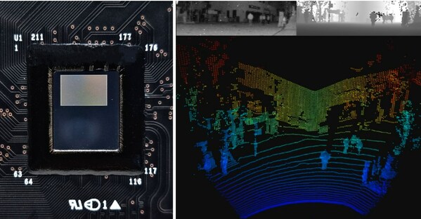
Fig. 1: Noise issues and resolution. Source: Flex Logix

In addition, noise affects both digital and analog systems. “Digital systems always start by digitizing data from some analog source, so digital systems start with all the same noise issues that analog systems do,” Jolly said. “In addition, digital systems must deal with quantization and pixelation issues, which always arise whenever some analog signal value is converted into a bit string. If the bits are then subjected to a lossy compression algorithm, this introduces additional noise. Furthermore, the increase in high-speed digital technologies such as double data rate memory (DDRx), quadrature amplitude modulation (QAM-x), non-return-to-zero (NRZ) line coding, pulse amplitude modulation (PAM), and other complex modulation schemes means that reflections and cross-channel coupling introduce noise into the system, possibly to the point of bit slipping and bit flipping. Many of these issues may be automatically handled by error correcting mechanisms within the digital protocol firmware or hardware.”
 
Noise can be introduced anywhere along the imaging chain and create a wide range of problems. “For example, the object being imaged may have shadows, occlusions, internal reflections, non-coplanarity issues, parallax, or even subtle vibrations, especially in a manufacturing environment,” Jolly explained. “In such situations, noise can complicate inspections. For example, a multi-layer circuit board being imaged with X-ray technology could have solder joint shadows if there are overlapping grid array components on the top and bottom of the board.”
 
Variability in the alignment between the image sensor and the subject of the image — rotational or translational offset, and planar skew — may add to the variability. And thermal gradients in the gap between the subject and the sensor may introduce noise, such as heat shimmer on a hot road. Low light and too-fast image capture also may introduce noise.
 
There are other issues to consider, as well. “A lens in the imaging chain may introduce noise, including chromatic aberration, spherical aberration, and errors associated with microscopic dust or lens imperfections. The lens controls the focus, depth of field, and focal plane of the image, all of which are key aspects of image acquisition. Finally, the imaging sensing hardware itself has normal manufacturing variability and thermal responses, even when operating in its specified range. A sensor with low resolution or low dynamic range is also likely to distort an image. Power integrity issues in the lines that power the sensor may show up as noise in the image. Finally, the camera’s opto-electronic conversion function (OECF) will play a key role in image quality,” Jolly added.
 
External sources of noise also can include flicker, which needs to be resolved for clear vision.

Fig. 2: Flicker from LED traffic lights or traffic signs poses a serious challenge for HDR solutions, preventing driver-assistance and autonomous driving systems from being able to correctly detect lighted traffic signs. Source: OmniVision

Imaging basics for ADAS 

While noise would seem to be a critical problem for ADAS sensors, given the potential for harm or damage, it’s actually less of an issue than for something like a consumer camera, where out-of-range pixels can ruin an image. ADAS is not concerned with aesthetics. It focuses on a binary decision — brake or not brake. In fact, ADAS algorithms are trained on lower-resolution images, and ignore noise that would be a product-killer in a consumer camera.

For example, to find a cat in the middle of an image, first the image is “segmented,” a process in which a bounding box is drawn around a potential object of interest. Then the image is fed into a neural net, and each bounding region is evaluated. The images are labeled, and then an algorithm can train itself to identify what’s salient. “That’s a cat. We should care about it and brake. It’s a skunk. We don’t care about it. Run it over,” said Katz. That may sound like a bad joke, but ADAS algorithms actually are trained to assign lower values to certain animals.

“It is about safety in the end, not so much ethics,” Katz said. “Even if someone does not care about moose, the car still has to brake because of the danger to the passengers. Hitting the brakes in any situation can pose a risk.” But higher values are assigned to cats and dogs, rather than skunks and squirrels.

If an object is fully or partly occluded by another object or obscured by light flare, it will require more advanced algorithms to correctly discern what it is. After the frame is received from the camera and has gone through basic image signal processing, the image is then presented to a neural net.

“Now you’ve left the domain of image signal processing and entered the domain of computer vision, which starts with a frame or sequence of frames that have been cleaned up and are ready for presentation,” said Katz. “Then you’re going to package those frames up and send them off to an AI algorithm for training, or you’re going to take those images and then process them on a local neural net, which will start by creating bounding boxes around each of the artifacts that are inside the frame. If the AI can’t recognize an object in the frame it’s examining, it will try to recognize it in the following or preceding frames.”

In a risky situation, the automatic braking system has about 120ms to respond, so all of this processing needs to happen within the car. In fact, there may not even be time to route from the sensor to the car’s own processor. “Here are some numbers to think about,” said Katz. “At 65 mph, a car is moving at 95 feet per second. At 65 mph, it takes about 500 feet to come to a complete stop. So even at 32.5 mph in a car, it will travel 47 feet in 1 second. If the total round trip from sensor to AI to brake took a half-second, you would be 25 feet down the road and still need to brake. Now keep in mind that the sensor is capturing images at about 30 frames per second. So every 33 milliseconds, the AI has to make another decision.”

In response, companies are using high-level synthesis to develop smart sensors, in which an additional die — with all the traditional functions of an image signal processor (ISP), such as noise reduction, deblurring, and edge detection — is sandwiched directly adjacent to the sensor.

“It’s now starting to include computer vision capability, which can be algorithmic or AI-driven,” said Katz. “You’ll start to see a smart sensor that has a neural net built inside. It could even be a reprogrammable neural net, so you can make updates for the different weights and parameters as soon as it gets smarter.”

If such a scheme succeeds, it means that a sensor could perform actions locally, allowing for real-time decisions. It also could repackage the information to be stored and processed in the cloud or car, for later training to increase accurate, rapid decision-making. In fact, many modern ISPs can already dynamically compensate for image quality. “For example, if there is a sudden change from bright light to low light, or vice-versa, the ISP can detect this and change the sensor settings,” he said. “However, this feedback occurs well before the image gets to the AI and object detection phase, such that subsequent frames are cleaner going into the AI or object detection.”

One application that already exists is driver monitoring, which presents another crucial noise issue for designers. “The car can have the sun shining right in your face, saturating everything, or the complete opposite where it’s totally dark and the only light is emitting off your dashboard,” said Bethurem. “To build an analog sensor and the associated analog equipment to have that much dynamic range and the required level of detail, that’s where noise is a challenge, because you can’t build a sensor of that much dynamic range to be perfect. On the edges, where it’s really bright or over-saturated bright, it’s going to lose quality, which has to get made up. And those are sometimes the most dangerous times, when you want to make sure the driver is doing what they’re supposed to be doing.”

AI and noise

The challenges of noise and the increasing intelligence of sensors have also attracted the attention of the AI community.

“There are already AI systems capable of filling in occluded parts of a digital image,” said Tony Chan Carusone, CTO at Alphawave Semi. “This has obvious potential for ADAS. However, to perform this at the edge in real-time will require new dedicated processing elements to provide the immediate feedback required for safety-critical systems. This is a perfect example of an area where we can expect to see new custom silicon solutions.”

Steve Roddy, chief marketing officer at Quadric, notes that path already is being pioneered. “Look at Android’s/Google’s ‘Magic Eraser’ functionality in phones – quickly deleting photo-bombers and other background objects and filling in the blanks. Doing the same on an automotive sensor to remove occlusions and ‘fill in the blanks’ is a known solved problem. Doing it in real time is a simple compute scaling problem. In 5nm technology today, ~10mm2 can get you a full 40 TOPs of fully programmable GPNPU capability. That’s a tiny fraction of the large (> 400 mm2) ADAS chips being designed today. Thus, there’s likely to be more than sufficient programmable GPNPU compute capability to tackle these kinds of use cases.”

Analyzing noise 

Analyzing noise in image sensors is a challenging and active area of research that dates back more than 50 years. The general advice from vendors is to talk to them directly to determine if their instrumentation aligns with a project’s specific needs.

“Noise is of a lot of interest to customers,” said Samad Parekh, product manager for analog/RF simulation at Synopsys. “There are many different ways of dealing with it, and some are very well understood. You can represent the noise in a closed form expression, and because of that you can very accurately predict what the noise profile is going to look like. Other mechanisms are not as well understood or are not as linear. Because those are more random, there’s a lot more effort required to characterize the noise or design with that constraint in mind.”

Best practices 

Keysight’s Jolly offered day-to-day advice for reducing and managing noise in image sensor projects:

  • Clearly define the objectives of the sensor as part of the overall system. For example, a slow, low-resolution thermal imager or vector network analyzer may reveal information about subcutaneous or subdural disease or injury that would be invisible to a high-resolution, high-speed visible light sensor. Work with your component and module vendors to understand what noise analysis and denoising they have already done. You will learn a lot and be able to leverage a lot of excellent work that has already been accomplished. Also, consider image noise throughout the total product life cycle and use simulation tools early in your design phase to minimize issues caused by sub-optimal signal integrity or power integrity.
  • Analyze the problem from the perspective of the end user. What are their objectives? What are their concerns? What skills do they possess? Can they make appropriate interventions and modifications? What is their budget? It may turn out, for example, that a fully automated system with a higher amount of noise may be more appropriate for some applications than a more complex system that can achieve much lower noise.
  • Become familiar with camera, optical, and imaging standards that are available, such as ISO 9358, 12232, 12233, 14524, and 15739, as well as European Machine Vision Association (EMVA) 1288.
  •  Investigate the latest research on the use of higher mathematics, statistics, and artificial intelligence in de-noising. Some of these techniques include expectation maximization estimation, Bayesian estimation, linear minimum mean square error estimation, higher-order partial differential equations, and convolutional neural networks.

Future approaches 

While current ADAS systems may tolerate more noise than other forms of imaging, that may not be the case in the future. A greater variety of use cases will push image sensors towards higher resolutions, which in turn will require more localized processing and noise reduction.

“A lot of the image processing in the past was VGA, but applications like internal cabin monitoring, such as eye-tracking the driver and passengers to recognize what’s going inside the cabin — including monitoring driver alertness or whether someone got left behind in the backseat — are going to start to drive us towards higher-resolution images,” Katz said. “In turn, that’s going to start to mandate increasing levels of noise reduction, dealing with image obstructions, and with being able to process a lot more data locally. When you go from VGA to 720 to 1020 up to 4k, you’re increasing the number of pixels you have to operate with by 4X. Every one of these demands more and more localized processing. That’s where we’ll end up going.”