Thursday, September 30, 2021

KT Imaging Files Patent Lawsuits against Apple, Microsoft, Google, Samsung, etc.

KT Imaging patent holding company believes that a number of companies infringed on its image sensor packaging patents. So, KT Imaging files the lawsuits against Apple, Microsoft, Google, Dell, Samsung, HP, AsusTek, Acer, etc.

AppleInsider publishes the case against Apple is published on Scribd. The patents in the case are 7,196,322, 7,511,261, 7,598,580, 8,004,602, and 8,314,481, filed for between 2004 and 2008 by Kingpak (Kingpak has been acquired by Tong Hsing two years ago.)

Wednesday, September 29, 2021

Gpixel Releases World’s Highest Resolution Global Shutter CMOS Sensor

Gpixel expands the GMAX product family of global shutter image sensors with the 152 MP GMAX32152, the highest resolution global shutter CMOS sensor commercially available in the market.

This latest GMAX sensor incorporates a 3.2 µm charge domain global shutter pixel in a 16556 (H) x 9200 (V) array for an imaging area of 53 mm x 29.4 mm (60.6 mm diagonal). The 1.8:1 wide aspect ratio optimizes the inspection of flat panel displays of similar format and increases the efficiency of large field of view aerial mapping applications.

GMAX32152 shares a common pixel and read-out architecture with the 103 MP GMAX32103, achieving the same full well capacity of 9.4 ke- and a read noise of 4 e- for a dynamic range of 67.6 dB.

The read out of image data is accomplished using 38 pairs of sub-LVDS channels each operating at 960 MHz delivering a full resolution frame rate of 16 fps at 12bit output and total aggregate data rate of 36.48 Gbps.

This sensor is provided in monochrome and RGB Bayer color options. Monochrome and RGB color engineering samples can be ordered today for delivery in October 2021, production release is expected by mid 2022.

Sony Unveils UV-Optimized Image Sensor

Sony announces the commercialization of the IMX487, a 2/3-type CMOS image sensor for industrial equipment, which is optimized for UV wavelength and comes with global shutter functionality and the industry’s highest (among UV sensors) pixel count of 8.13MP.

The sensor captures UV light with high efficiency made possible by the industry’s smallest (among UV sensors) 2.74 µm pixel size. It utilizes Sony’s Pregius S global shutter technology, which employs a unique back-illuminated pixel structure on a stacked CMOS image sensor,

Sony expects the new sensor to be useful in a variety of applications, including semiconductor pattern defect inspection in the existing UV camera market, thereby contributing to improving productivity in manufacturing processes and helping to solve industrial issues.

In general, UV cameras enable sorting of materials that would be difficult in visible light, as well as checking for minute scratches and defects on the surface of objects. They have conventionally been used in semiconductor pattern defect inspection; however, to expand the scope of application in the future, demand has continued to grow for an image sensor that not only provides sensitivity in the UV wavelength, but also delivers high resolution, low noise, and high-speed performance.

Pixel with Nearly Unity-Gain SF

IEEE Sensors publishes a video presentation of Xiaoliang Ge and Albert Theuwissen (Delft University) paper "A CMOS Image Sensor with Nearly Unity-Gain Source Follower and Optimized Column Amplifier."

"This paper presents a CMOS image sensor with in-pixel nearly unity-gain pMOS transistor based source followers and optimized column-parallel amplifiers. The prototype sensor has been fabricated in a 0.18 µm CMOS process. By eliminating the body effect of the source follower transistor, the voltage gain for the pixel-level readout circuitry approaches unity. The use of a single-ended common-source cascode amplifier with ground rail regulation improves the PSRR of the column-parallel analog front-end circuitry and further the noise performance. The prototype sensor with proposed readout architecture reaches a 1.1e- input-referred temporal noise with a column-level ×16 analog gain."

Syntiant Partners with Pixart on Low Power Always-On Applications

GlobeNewswire: Competing with Himax WiseEye always-on IoT platform, Pixart partners with Syntyant neural processing startup to come up with a joint low power vision platform.

Syntiant introduces its Syntiant® NDP200 Neural Decision Processor (NDP), the company’s first chip designed for vision processing that can provide highly accurate inference at under 1mW.

The NDP200 can run multiple applications simultaneously with minimal power consumption, including AI vision features such as person detection, object classification, motion tracking and occupancy monitoring.

Our NDP200 brings extraordinary inference capabilities to a wide variety of always-on image and sensor applications,” said Kurt Busch, CEO of Syntiant. “Our Core 2 architecture minimizes data movement by coupling memory and MAC functions that generally provides 100x improvement in efficiency and performance. As an example, an application that lasts three and a half days on a battery-powered device using an Arm A53 processor would last one year running on the NDP200.

The combination of Syntiant’s NDP200 and PixArt's ultra-low-power image sensor offers the ability to develop highly accurate person and object detection systems that consume very little power with almost no latency,” said Sen Huang, CEO of PixArt Imaging. “These features are extremely critical to the growing need for imaging sensor applications found in battery-operated IoT devices, such as video doorbells and security cameras.”

IntoPIX Announces IP Cores for 10x Raw Image Data Compression

BusinessWire: IntoPIX announces the extension of its range of TICO RAW IP-cores supporting additional pixel per clock architectures to target more devices and more sensor types.

Integrated on ASIC or in small FPGAs, these IP-cores cover the most popular CFA Bayer patterns, sensor bit-depths from 10 up to 16 bits and resolutions from 1MP up to 100MP.

TICO-RAW is the new RAW. It preserves access to the control over white balance, exposure and color grading with the world's best efficiency. “The continued use of regular RAW files means that the ultimate image quality can’t be maintained without creating monster-size files or using too much bandwidth,” explains Jean-Baptiste Lorent, Marketing and Sales Director at intoPIX. With 10 times less bandwidth required and 10 times less storage needed compared with those of regular RAW, TICO-RAW offers a high speed and low complexity.

Monday, September 27, 2021

Strategy Analytics on H1 2021 Smartphone CIS Market

Strategy Analytics estimates that Sony has captured 42% smartphone CIS market share in H1 2021 and 41% in Q2 2021. The whole smartphone CIS market grew 10% YoY in H1:

"The global smartphone Image sensor market in H1 2021 clocked a total revenue of $7 billion.

This Strategy Analytics research report finds that the smartphone image sensor market managed to record a revenue growth of more than 10 percent year-over-year in H1 2021.

The report estimates that the top three vendors took almost 80 percent revenue share in the global smartphone image sensor market in H1 2021.

Jeffrey Mathews, Senior Analyst at Strategy Analytics says, “The image sensor vendors witnessed an accelerated momentum from smartphone OEMs, who actively adopted high-resolution CIS and low-pixel CIS products for multicamera applications, to secure inventory and cater to pent-up demand. Sony, Samsung and OmniVision supplied key high-resolution CIS products to leading smartphone OEMs in H1 2021.”

Stephen Entwistle , Vice President of the Strategic Technologies Practice at Strategy Analytics commented, “The introduction of new high-resolution and large format CIS products from the major vendors are expected to boost the revenue opportunities in the market. However, we note that the supply fluctuations of various high-pixel and low pixel CIS products continue to challenge the growth prospects of the smartphone image sensor market.

Low Noise SPAD in 180nm Process

IEEE Journal of Selected Topics in Quantum Electronics publishes EPFL and KIST paper "A Low-noise CMOS SPAD Pixel with 12.1 ps SPTR and 3 ns Dead Time" by Francesco Gramuglia, Ming-Lo Wu, Claudio Bruschini, Myung-Jae Lee, and Edoardo Charbon.

"Single-photon avalanche diodes (SPADs) have become the sensor of choice in many applications whenever high sensitivity, low noise, and sharp timing performance are required, simultaneously. Recently, SPADs designed in CMOS technology, have yielded moderately good performance in these parameters, but never equaling their counterparts fabricated in highly customized, non-standard technologies. The arguments in favor of CMOS-compatible SPADs were miniaturization, cost and scalability. In this paper, we present the first CMOS SPAD with performance comparable or better than that of the best custom SPADs, to date. The SPAD-based design, fully integrated in 180 nm CMOS technology, achieves a peak photon detection probability (PDP) of 55% at 480 nm with a very broad spectrum spanning from near ultraviolet (NUV) to near infrared (NIR) and a normalized dark count rate (DCR) of 0.2 cps/µm^2, both at 6V of excess bias. Thanks to a dedicated CMOS pixel circuit front-end, an afterpulsing probability of about 0.1% at a dead time of ∼3 ns were achieved. We designed three SPADs with a diameter of 25, 50, and 100 µm to study the impact of size on the timing jitter and to create a scaling law for SPADs. For these SPADs, a single-photon time resolution (SPTR) of 12.1 ps, 16 ps, and 27 ps (FWHM) was achieved at 6 V of excess bias, respectively. The SPADs operate in a wide range of temperatures, from -65◦C to 40◦C, reaching a normalized DCR of 1.6 mcps/µm^2 at 6 V of excess bias for the 25 µm at -65◦C."

Sunday, September 26, 2021

Galaxycore 12-inch BSI Facility to Start Production in 2 Years

Laoyaoba: Galaxycore says on the investor interaction platform that the company's 12-inch CIS BSI facility construction is progressing smoothly, and the main building has been capped on August 16. The company expects to start the production in 2 years. The fab capacity is 20,000 wafers per month.

In 2018, 2019 and 2020, the gross profit margin of Galaxycore's CMOS sensors was 25.32%, 27.50% and 28.54%, respectively which is similar to or even higher than that of its competitors. Galaxycore is confident in the competitiveness of its new high-end products in development now.

Saturday, September 25, 2021

Open Letter from Junichi Nakamura, New President of the International Image Sensor Society

Open Letter from the New President

Dear all,

This time, I was elected as a new President of International Image Sensor Society (IISS) by the IISS Board of Directors at the Board meeting just after the 2021 International Image Sensor Workshop (IISW) closure. It is my great pleasure and honor to serve as President of IISS and I will try my best to improve services of IISS/IISW.

As was mentioned at the very beginning of the 2021 IISW by Johannes Solhusvik, the General Chair of the 2021 IISW, the key concept of the IISW is to provide an opportunity to exchange the latest progress in image sensor and related R&D activities to the top image sensor technologists in the world in an informal atmosphere. This concept was conceived by Eric Fossum, the Founder of this series of workshop, at the very first workshop in 1986 (named “IEEE Workshop on CCDs”), and has been realized and enhanced by the three former Presidents of IISS, Eric, Nobukazu Teranishi and Albert. This will be kept in the future workshop.

With the retirement of Eric, Nobu and Albert from the Board, the Board of Directors has invited three very strong image sensor technologists to the Board, namely, Boyd Fowler (OmniVision, USA), Robert Henderson (University of Edinburgh, UK) and Yusuke Oike (Sony, Japan). Please join me in welcoming them to the Board of IISS.

Finally, I would like to express my sincere gratitude to the three Co-Founders/former Presidents of IISS for their enthusiasm to “bring the imaging community to a higher level”. The IISS Directors will inherit this spirit. I hope Eric, Nobu and Albert can continue giving us any suggestions and insights as members of the newly established Governance Advisory Committee.

Best regards,

Junichi Nakamura
President of IISS
CTO of Brillnics Inc.

STA Founder Dick Bredthauer Passed Away

As posted in CCD-World mailing list, Semiconductor Technology Associates, Inc. founder Dick Bredthauer passed away.

Dr. Richard Bredthauer was involved in the design and fabrication of a large variety of scientific imaging CCDs from 1975 to 2016. He managed CCD development at Lockheed Martin, Loral, Ford Aerospace, and Rockwell.  He designed the original 9k x 9k imager while at Lockheed Martin, and his CCDs included notable instruments such as Hubble’s WFPC2, all of the visible imagers on Cassini, the stereo camera in Mars Pathfinder, and most recently the lightning imager for GOES-R. In 2016, his son Dr. Greg Bredthauer became president of STA and took over daily operations.


Thanks to GM for the pointer!

Friday, September 24, 2021

Open Letter from Albert Theuwissen

OPEN LETTER TO THE INTERNATIONAL IMAGE SENSOR SOCIETY.

Dear all,

Yesterday (Thursday 23/09/2021) the International Image Sensor Workshop 2021 came to an end. Immediately after the workshop closure we had a meeting with the Board of Directors of the International Image Sensor Society. In that meeting Eric Fossum, Nobukazu Teranishi and Albert Theuwissen (the three co-founders of IISS) announced their retirement from the Board. The retired members will set up a Government Advisory Committee (without any voting rights anymore), but they will be no longer directly involved in the organization of the IISW.

If I speak for myself : it was a great honour and even a greater pleasure for me to work for and to work with Eric, Nobu and all other Board members. This is a group of people that constantly tries to bring the imaging community to a higher level. Imaging has given and still gives me a lot of joy, motivation, strength in my professional live and last but not least also in my private life it brought us a nice piece of bread on our table. So for me it was very normal to give something back to our imaging community by means of my activities in IISS.

Over the years I learned a lot from my involvement in IISS, about how to work with various cultures, how to work with world-level top-experts in the field and how to work with individuals that all have a strong character (otherwise they would not have climbed up to the level where they now are). And very often the cooperation with my Board colleagues put myself in front of the mirror which led to some self-reflection.

I wish IISS and all Board members all the best in the coming future. It is now up to the next generation to manage IISS and I am more than confident that the next generation will succeed. But if needed, they always can count on me for advice.

Best regards from Belgium.

Albert, former president of IISS.

24/09/2021.

IDQ Photon Sensors - from Mobile Phones to Space Launchers

Física Exactas UBA publishes a presentation "Quantum technologies for mobile phones and space launchers" by Félix Bussières ID Quantique SA, Switzerland:

Galaxycore Evaluates its 32MP Sensor Engineering Samples

DailyEconomicNews: In line with its intentions to penetrate mid- to high-end CIS market, Galaxycore announces at the investor interactive platform on September 24: "Dear investors, hello. The company's high-end pixel research and development is progressing smoothly, and the CMOS image sensor with 32 million pixels and above has entered the stage of internal evaluation of engineering samples. Thank you for your attention!"

Smartsens Announces Three BSI Global Shutter Sensors

CoreIntelligenceSmartSens launches three new SmartGS-2 series image sensors-SC350HGS / SC650HGS / SC950HGS with 3MP to 9MP resolutions aimed to industrial cameras for intelligent applications. the QE of the three products reaches 90% at 520nm.

Samples of the three sensors are available now, and mass production is expected to start in Q4 2021.

Thursday, September 23, 2021

Excess Noise Reduction in APDs

IEEE Journal of Selected Topics in Quantum Electronics publishes a paper "Evolution of Low-Noise Avalanche Photodetectors" by Joe C. Campbell from University of Virginia.

"This paper reviews materials and structural approaches that have been developed to reduce the excess noise in avalanche photodiodes and increase the gain-bandwidth product."

"It has been shown for a wide range of materials including InP, GaAs, In1-xAlxAs, Si, AlxGa1-xAs, SiC, GaP, and GaInP that reducing the thickness of the multiplication layer, usually to submicron dimensions, results in lower excess noise. This is contrary to expectations based on the local-field model and points to its inadequacy when the non-local nature of impact ionization becomes significant."

Assorted Videos: Trinamix, Vision Research, Immervision, Teledyne-e2v, Cepton

Trinamix expands its multispectral 3D imaging applications with smartphone behind OLED face recognition and driver monitoring:


Vision Research promotes its fast BSI sensors:


Immervision publishes its SPIE Optical Systems Design International Symposium presentation on freeform lenses in consumer applications:


Teledyne-e2v promotes its linescan sensors:


Autosens publishes interviews with Cepton:

Wednesday, September 22, 2021

SPADs in Globalfoundries' 55nm BCD Process

It appears that Globalfoundries becomes a viable option for SPAD-based sensors. At least, three Globalfoundries' employees are co-authors of the following paper:

IEEE Journal of Selected Topics in Quantum Electronics publishes a paper "Engineering Breakdown Probability Profile for PDP and DCR Optimization in a SPAD Fabricated in a Standard 55nm BCD Process" by Francesco Gramuglia, Pouyan Keshavarzian, Ekin Kizilkan, Claudio Bruschini, Shyue Seng Tan, Michelle Tng, Elgin Quek, Myung-Jae Lee, and Edoardo Charbon from EPFL (Switzerland), Globalfoundries (Singapore), KIST (Korea).

"In this paper, we present SPADs based on DPW/BNW junctions in a standard Bipolar-CMOS-DMOS (BCD) technology with results comparable to the state-of-the-art in terms of sensitivity and noise in a deep sub-micron process. Technology CAD (TCAD) simulations demonstrate the improved PDP with the simple addition of a single existing implant, which allows for an engineered performance without modifications to the process. The result is an 8.8 μm diameter SPAD exhibiting ~2.6 cps/μm^2 DCR at 20°C with 7 V excess bias. The improved structure obtains a PDP of 62 % and ~4.2 % at 530 nm and 940 nm, respectively. Afterpulsing probability is ~0.97 % and the timing response is 52 ps FWHM when measured with integrated passive quench/active recharge circuitry at 3V excess bias."

PAM4 in Image Sensor-based Communication

PAM4 signalling has been adopted in many recent high speed interfaces, such as PCIe 6.0, MIPI A-PHY, Auto-Serdes, and many others. In the following OSA paper, PAM4 is being proposed for image sensor based communication:

"PAM4 rolling-shutter demodulation using a pixel-per-symbol labeling neural network for optical camera communications" by Yun-Shen Lin, Chi-Wai Chow, Yang Liu, Yun-Han Chang, Kun-Hsien Lin, Yi-Chang Wang, and Yi-Yuan Chen from National Yang Ming Chiao Tung University, National Chiao Tung University, and Industrial Technology Research Institute, Taiwan, with Philips Hong Kong.

"The typical optical camera communication (OCC) modulation scheme is based on binary intensity modulation. To increase the transmission data rate, multi-level modulation format is highly desirable. In this work, we bring forward and demonstrate a rolling shutter 4-level pulse amplitude modulation (PAM4) demodulation scheme for OCC systems using pixel-per-symbol labeling neural network (PPSL-NN) for the first time up to the authors’ knowledge. A bit-rate distance product of 28.8 kbit/s • m per color is achieved. The proposed scheme is to calculate and re-sample the pixel-per-symbol (PPS) to make sure the same number of pixels in each PAM4 symbol is corresponding to a label for the neural network. Experiment results reveal that the proposed scheme can efficiently demodulate high speed PAM4 signal in the rolling shutter OCC pattern."

Tuesday, September 21, 2021

New Imaging Technologies Video

New Imaging Technologies (NIT) presents its SWIR and HDR sensors in this video:


Recently, NIT has been awarded with a large funding program by the French Government for improving and industrializing its in-house hybridization technology, paving the way to very small infrared sensor pitch. The so called NH technology allows to perform a 3D stack of a read out circuit with a photodiode array without using the traditional Indium bump bonding technique. The NH yield is extremely high and with this investment program it is expected to reach pixel pitch of less than 5um.

Galaxycore CEO on Growth of China Semiconductor Industry

PerceptionCoreVision publishes a transcript of Galaxycore CEO Zhao Lixin (Stanly Zhao) talk at the 2nd Shanghai Free Trade Zone Lingang New Area Semiconductor Industry Development Forum held on September 15, 2021. Few quotes:

"China has a lot to do in the development of image sensors. From the perspective of sales volume, Galaxycore plus Omnivision's CIS shipments account for more than 50% of the world; from the perspective of value, Gekewei’s 1 billion plus Howe 2 billion, accounting for about 16% of the global 20 billion CIS market.

I often proudly say that our Galaxycore is good. Why is Galaxycore good? We, Galaxycore, were the largest domestic customer of SMIC, the largest foundry in China in 2007. During the financial crisis in 2008, we placed an order of 100,000 8-inch wafers for SMIC. Of course, we were surpassed by HiSilicon, because HiSilicon was too powerful.

Before that, Galxycore has been the top four customers of SMIC, and we are also the major customers of packaging factories such as Changjiang Electronics, Jingfang and Huatian. Therefore, only after you have a large scale can you promote the national economy and support the development of this industry. Therefore, I put a lot of emphasis on the shipment volume of a wafer, the Internet emphasizes traffic, and semiconductor companies must emphasize the use of silicon wafers. Galaxycore currently ranks among the top three in terms of silicon wafer usage in China.

The second is to focus on high-end, because only ICs on high-end brand mobile phones have sufficient scale and profits. Without profit, there is no way to do high-end R&D. Therefore, to drive the development of the entire industry chain in China, there must be sufficient profits. Just like a company like Huawei, its high-end mobile phone camera supports three world-renowned companies, Sony, Largan and Sunny. So it can feed so many people with a single chip. But if you can't do high-end, it is unlikely to be profitable.

The development of China's semiconductor industry still requires the use of mobile phones to drive our chip design companies. Design companies drive Foundry factories, packaging factories, and then equipment manufacturers and material manufacturers.

Why can Galaxycore do well? Because Galaxycore is unique in process research and development. Therefore, in order to speed up the research and development of high-end products, we must build our own factories to do the research and development of special processes. Now Lingang is a very good place, so we invested 2.2 billion US dollars in Lingang to build a world's most advanced characteristic process line.

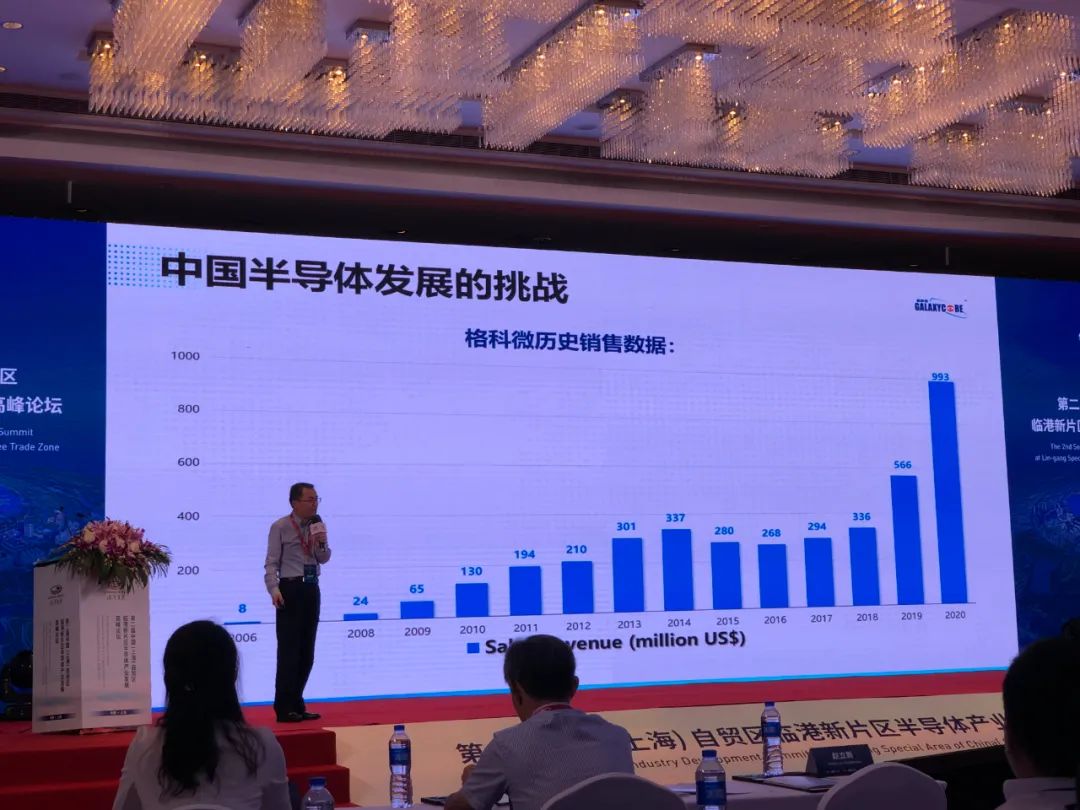
Based on this sales data of Galaxycore, I will tell you about our development history. You can see that from 2006 to 2007, it was the research and development period. In 2008, a large number of shipments were made. In 2009, despite the financial crisis, our business doubled.

In 2014, we made about 340 million U.S. dollars. At this time, we were stuck overseas because we couldn't make BSI crafts. Because the neck of BSI was stuck, we couldn't make high-end products. Then we will cooperate with Samsung around 2016 and 2017 to make our BSI products. At this time, the company's performance is developing by leaps and bounds. Last year we approached 1 billion US dollars.

When there is a breakthrough in research and development, this performance is relatively easy to grow rapidly, and the shipment volume is also amazing. We have achieved shipments of nearly 2.4 billion units. With this scale, we will be able to do more high-end designs later."

Monday, September 20, 2021

Samsung 200MP Sensor Video

Samsung publishes a promotional video about its 200MP HP1 sensor:

Dark Current Reduction in Small Pixels

Seoul National University of Science and Technology publishes a MDPI paper "Reduction of Fluorine Diffusion and Improvement of Dark Current Using Carbon Implantation in CMOS Image Sensor" by Su-Young and Sung-Hoon Choa.

"Recently, the demand of a high resolution complementary metal-oxide semiconductor (CMOS) image sensor is dramatically increasing. As the pixel size reduces to submicron, however, the quality of the sensor image decreases. In particular, the dark current can act as a large noise source resulting in reduction of the quality of the sensor image. Fluorine ion implantation was commonly used to improve the dark current by reducing the trap state density. However, the implanted fluorine diffused to the outside of the silicon surface and disappeared after annealing process. In this paper, we analyzed the effects of carbon implantation on the fluorine diffusion and the dark current characteristics of the CMOS image sensor. As the carbon was implanted with dose of 5.0 × 10^14 and 1 × 10^15 ions/cm2 in N+ area of FD region, the retained dose of fluorine was improved by more than 131% and 242%, respectively than no carbon implantation indicating that the higher concentration of the carbon implantation, the higher the retained dose of fluorine after annealing. As the retained fluorine concentration increased, the minority carriers of electrons or holes decreased by more Si-F bond formation, resulting in increasing the sheet resistance. When carbon was implanted with 1.0 × 10^15 ions/cm2, the defective pixel, dark current, transient noise, and flicker were much improved by 25%, 9.4%, 1%, and 28%, respectively compared to no carbon implantation. Therefore, the diffusion of fluorine after annealing could be improved by the carbon implantation leading to improvement of the dark current characteristics."

Sunday, September 19, 2021

Event Cameras Literature Review

Hong Kong University of Science and Technology publishes Jianhao JIAO's slides "Literature Review on Event Cameras" based on Zurich University paper "Event-based Vision: A Survey" by Guillermo Gallego, Tobi Delbruck, et al. Few  slides from the presentation:

Friday, September 17, 2021

Melexis Integrates 940nm Bandpass Filter on Top of its iToF Sensor

Melexis has developed a new version of its time-of-flight 3D camera MLX75026 with a fully integrated infrared bandpass (IRBP) filter. By integrating the IRBP, it is no longer required to include a separate IR filter in the lens or sensor assembly. This solution is said to be unique in the industry. It reduces design complexity and cost, while creating more design choice when sourcing a lens.

An IR filter is mandatory in every ToF application to reduce out-of-band infrared light in the operating environment, which could otherwise lower the dynamic range of the sensor,” explained Gualtiero Bagnuoli, Optical sensors marketing manager at Melexis. “A separate filter adds cost and complexity to a design, but by using the MLX75026 with IRBP filter, engineers can avoid both the cost and complexity, and explore the benefits of time-of-flight sensing more easily.

The integration of the correct IR bandpass filter is not trivial: the passband must be adapted to the illumination and the filter shall accept light from a wide range of incidence at minimal spectral shift (optically hard filter). This facilitates the usage of ToF-lenses with high apertures (low f-number). Melexis is the only ToF sensor manufacturer currently offering this option, which is now available as a variant of the MLX75026.

MLX75026 with IRBP filter has QVGA (320x240 pixels) resolution with a 1/4 inch optical format and supports 940 nm illumination. Samples of the MLX75026 with IRBP filter are available now.

ST Presents its First iToF Sensor at ESSCIRC

ST has presented its first iToF image sensor at 47th European Solid-State Circuits Conference being held this week in a virtual space:

"4.6μm Low Power Indirect Time-of-Flight Pixel Achieving 88.5% Demodulation Contrast at 200MHz for 0.54MPix Depth Camera"
by Cedric Tubert, Pascal Mellot, Yann Desprez, Céline Mas, Arnaud Authié, Laurent Simony, Grégory Bochet, Stephane Drouard, Jeremie Teyssier, Damien Miclo, Jean-Raphael Bezal, Thibault Augey, Franck Hingant, Thomas Bouchet, Blandine Roig, Aurélien Mazard, Raoul Vergara, Gabriel Mugny, Arnaud Tournier, Frédéric Lalanne, Francois Roy, Boris Rodrigues Goncalves, Matteo Vignetti, Pascal Fonteneau, Vincent Farys, Francois Agut, Joao Miguel Melo Santos, David Hadden, Kevin Channon, Christopher Townsend, Bruce Rae, and Sara Pellegrini.

"In this paper, a 4.3e- RMS low noise 4.6μm Time-of-Flight pixel based on charge domain with kTC noise removal is proposed to enhance the depth camera image quality. The pixel takes advantages of 6μm gradually doped epitaxial layer for 88.5% demodulation contrast at 200MHz and 18.5% QE at 940nm. Buried channel transfer gates are used to enable low capacitive switching and allowing best-in-class 1.4μW/pixel power consumption at 200MHz. The pixel is fully isolated due to deep trench isolation and pixel bulk is biased at several hundreds of mV for ultimate low power Time-of-Flight sensor and system. The paper describes the design of 0.54Mpix camera (672 x 804 pixels) implementing demodulation circuits robust against EMI and multi-devices interferences. The performance of an indirect Time-of-Flight system is demonstrated with 1.0% depth noise under 40kLux at 30fps."

ST kindly sent me a few slides from the presentation:


Other ESSCIRC imaging papers are:

  • "Advancements in Indirect Time of Flight Image Sensors in Front Side Illuminated CMOS"
    Markus Dielacher, Martin Flatscher, Reinhard Gabl, Richard Gaggl, Dirk Offenberg, and Jens Prima from Infineon and PMD
    "We will present major advances in Time of Flight image sensors for consumer applications. Several innovative elements integrated into a 130nm front side illumination CMOS node reveal superior sensor performance so far only attributed to much more complex backside illumination technologies. The gate controlled pixels comprising deep trenches, buried mirrors and integrated prisms, reveal high quantum efficiency and modulation transfer function close to the physical pixel size. In-pixel common mode suppression prevents saturation even under backlight conditions. The comprehensive System on Chip integrates high speed ADCs, a flexible phase shifter, as well as current monitoring for laser safety."
  • "Dark Count Rate in Single-Photon Avalanche Diodes: Characterization and Modeling Study"
    Mathieu Sicre, Megan Agnew, Christel Buj, Jean Coignus, Dominik Golanski, Rémi Helleboid, Bastien Mamdy, Isobel Nicholson, Sara Pellegrini, Denis Rideau, David Roy, and Francis Calmon from CEA-Leti, INSA Lyon, STMicroelectronics.
    "Dark Count Rate (DCR) in Single-Photon Avalanche Diodes (SPAD) in Complementary Metal-Oxide Semiconductor technology is characterized and analyzed with a comprehensive simulation methodology. Based on a series of measurements of SPAD with various architectures, on an extended range of voltages and temperatures, the DCR measurements are correlated to the spatial localization of traps within the device and their parameters. To this aim, process and electrical simulations using Technology Computer-Aided Design (TCAD) tools are combined with an in-house McIntyre solver to compute the breakdown probability (Pt). The traps are accounted for using thermal SRH carrier generation-recombination mechanism which is coupled with the position-dependent breakdown probability. This rigorous methodology makes it possible to directly compare with DCR measurements, since only generated carriers with a non-negligible avalanche probability are considered."
  • "A High-Speed Low-Power Sun Sensor with Solar Cells and Continuous Operation"
    Rubén Gómez-Merchán, María López-Carmona, Juan Antonio Leñero-Bardallo, Ángel Rodríguez-Vázquez from Universidad de Sevilla-IMSE-CNM CSIC, Spain.
    "A novel sun sensor concept is presented. Photodiodes operating as solar cells with continuous operation and dedicated logic to calculate the centroid position are integrated to achieve lower latency and energy consumption. The output data flow is remarkably reduced because the centroid of the illuminated pixels is the only sensor output data. It overcomes conventional digital sun sensors based on Active Pixel Sensor (APS) pixels and Address Event Representation (AER) in terms of latency and power consumption. Its latency is in the order of microseconds with an average power consumption lower than 100 uW. Experimental results are provided and benchmarked."
  • "A 0.94-μVrms Input Noise Pixel-Level Continuous Time ΣΔ IADC Interface for THz Sensing"
    Gabriele Quarta, Matteo Perenzoni, Stefano D'Amico from Fondazione Bruno Kessler and Università Del Salento, Italy
    "The goal of this work is the design, realization, and characterization of a pixel-level front-end in 0.15μm CMOS technology, that allows to directly convert in the digital domain the weak output signal from the Field-Effect Transistor (FET) TeraHertz (THz) detector, in a noise-efficient way. The chosen architecture is a Continuous-Time Sigma-Delta Incremental Analog-to-Digital Converter (CT ΣΔ IADC) with a current DAC feedback, chopper technique and digital lock-in modulation. The measured SNR of this interface is 67.45dB, corresponding to an equivalent number of bit (ENOB) of 10.91. The pixel readout area is 0.072mm2, and the power consumption is 65μW from 1.8V supply. The Noise Equivalent Power (NEP) of the THz detector and readout chain is 268pW/√𝐇𝐳. The readout channel Input Referred Noise (IRN) is 1.2μVrms with the FET, and 0.94μVrms for the channel without detector.
  • "The Essential Contribution of CMOS Imaging Technologies to Earth Observation Applications"
    Pierre Magnan, ISAE-SUPAERO, France
    "In this paper we discuss how the high performances CMOS imaging process improvements, strongly driven by consumer market’s needs, has allowed this technologies to pop-up in the field of Earth Observation instruments traditionally making use of dedicated Charge Coupled Devices (CCD). After reviewing the various Earth image captures techniques and related sensor architectures, the specific requirements on the sensor process will be examined and it will be shown how modern CMOS imaging process, although developed initially for high volume small pixel pitch application, can efficiently fulfill these needs, even allow new performances level, and thanks to additional features enable new achievements particularly suited to the New Space context."
  • "Luximos: a 768x64 900-fps Tileable Pipelined X-Ray CMOS Image Sensor for Dental Imaging with 2.6 LSB/nGy Sensitivity"
    Nicola Massari, Xu Hesong, Alessandro Tarolli, Luca Parmesan, Daniele Perenzoni, Sabrina Colpo, Nicola Fronza, David Stoppa, Matteo Perenzoni, Alfredo Maglione from AdvanSid, FBK, and AMS
  • "Comprehensive Modeling and Characterization of Photon Detection Efficiency and Jitter in Advanced SPAD Devices"
    Rémi Helleboid, Denis Rideau, Isobel Nicholson, Norbert Moussy, Olivier Saxod, Marie Basset, Jérémy Grebot, Antonin Zimmerman, Bastien Mamdy, Dominik Golanski, Megan Agnew, Sara Pellegrini, and Mathieu Sicre from CEA-Leti, STMicroelectronics, INRIA
  • "High Tuning Range Spiking 1R-1T VO2 Voltage-Controlled Oscillator for Integrated RF and Optical Sensing"
    Teodor Rosca, Fatemeh Qaderi, and Adrian Mihai Ionescu from EPFL
    "In this work we propose and experimentally validate a relaxation oscillator architecture with ultra-high tuning range (higher than 400%, from 5KHz to more than 25kHz when the control voltage is varied from 2.5 to 5V) that exploits the reversible metal-insulator transition in 2-terminal Vanadium Dioxide thin film devices loaded to a MOSFET common source amplifier. We propose and validate an analytical model that connects key output signal metrics to the intrinsic properties of the phase-change VO2 device employed. In addition, we demonstrate RF and optical sensing capabilities, with sensitivities of 4.64 Hz/dBm and 4.23 Hz/mW to RF and Optical Power, respectively."