Wednesday, May 31, 2023

VoxelSensors Raises €5M in Seed Funding for blending the physical and digital worlds through 3D perception

Press release:
https://voxelsensors.com/wp-content/uploads/2023/05/VoxelSensors_Announces_Seed_Round_Closing_May-17-2023-_-RC_FINAL.pdf

Brussels (Belgium), May 17, 2023
- VoxelSensors today announces an investment of €5M led by Belgian venture capital firms Capricorn Partners and Qbic, with participation from the investment firm finance&invest.brussels, existing investors and the team. VoxelSensors’ Switching Pixels® Active Event Sensor (SPAES) is a novel category of ultra-low power and ultra-low latency 3D perception sensors for Extended Reality (XR)1 to blend the physical and digital worlds. The funding will be used to further develop VoxelSensors’ roadmap, hire key employees, and strengthen business engagements with customers in the U.S. and Asia. Furthermore, VoxelSensors remains committed to raising funds in order to back its ambitious growth plans.

Extended Reality device manufacturers require low power consumption and low latency 3D
perception technology to seamlessly blend the physical and digital worlds and unlock the true
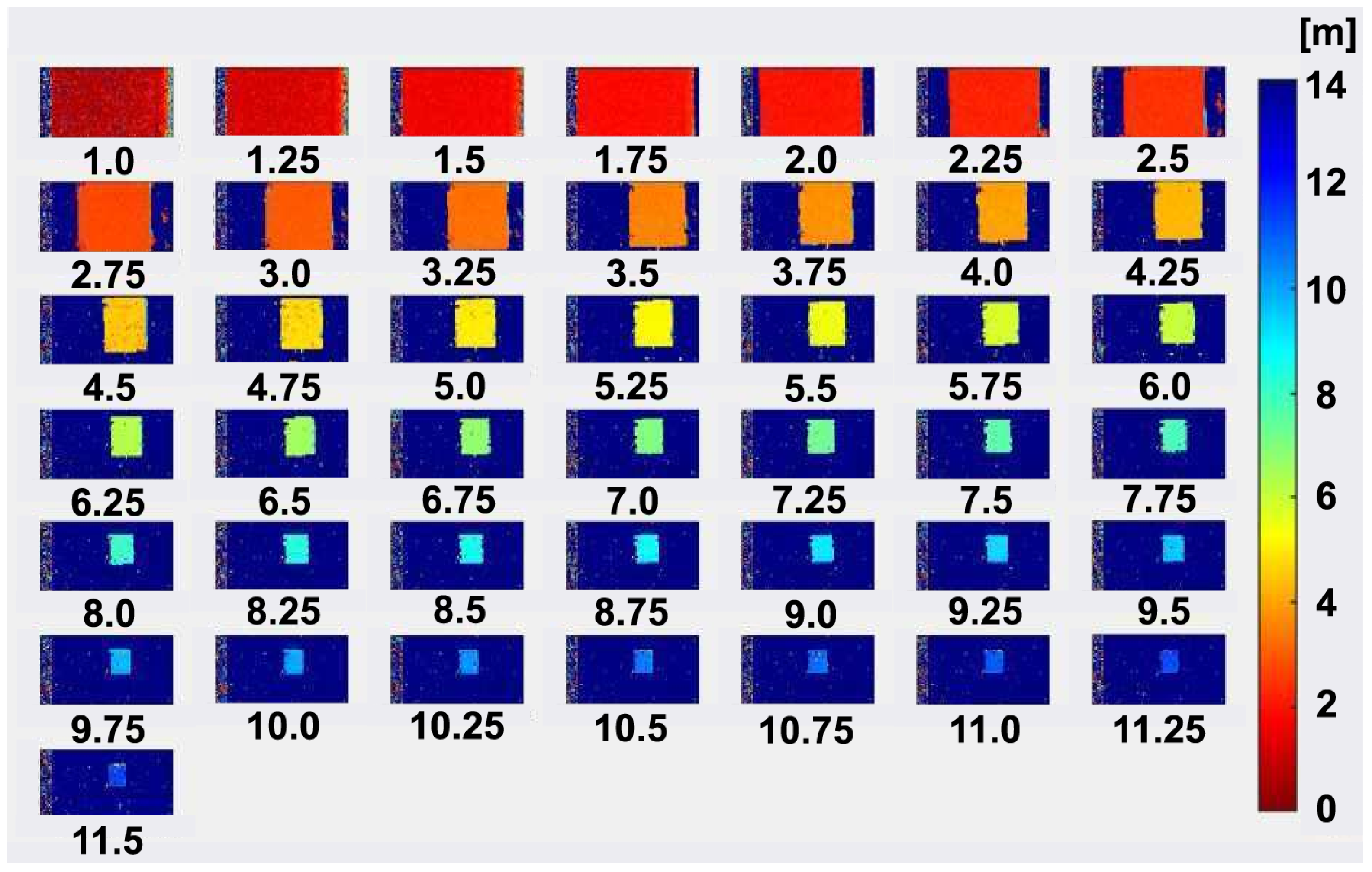
potential of immersive experiences. VoxelSensors’ patented Switching Pixels® Active Event Sensor technology has uniquely resolved these significant 3D perception challenges and is the world’s first solution reaching less than 10 milliwatts power consumption combined with less than 5 milliseconds latency while being resistant to outdoor lighting at distances over 5 meters and being immune to crosstalk interferences.

The founders of VoxelSensors boast a combined experience of more than 50 years in the development of cutting-edge 3D sensor technologies, systems and software. Their track record of success includes co-inventing an efficient 3D Time of Flight sensor and camera technology, which was acquired by a leading tech company.

“Our goal at VoxelSensors is to seamlessly integrate the physical and digital worlds to a point level where they become indistinguishable,” said Johannes Peeters, co-founder and CEO of VoxelSensors. "Extended Reality has rapidly gained traction in recent years, with diverse applications across sectors such as gaming, entertainment, education, healthcare, manufacturing, and more. With our Switching Pixels® Active Event Sensor technology we are poised to deliver unparalleled opportunities for groundbreaking user experiences. We are excited by the opportunity to contribute to the growth of our growing industry and honored by the trust of these investors to help us expand the company and accelerate market penetration.”

“We are excited to invest with the Capricorn Digital Growth Fund in VoxelSensors. We appreciate the broad experience in the team, the flexibility of the 3D perception solution towards different applications and the solid intellectual property base, essential for the success of a deep tech start-up. The team has a proven track record to build a scalable business model within a Europe-based semiconductor value chain. We also highly value the support of the Brussels region via Innoviris,” explained Marc Lambrechts, Investment Director at Capricorn Partners.

“As an inter-university fund, Qbic is delighted to support VoxelSensors in this phase of its journey. It’s a pleasure to see the team that led one of Vrije Universiteit Brussels’ (VUB) most prominent spinoffs to successful exit, start another initiative in this space. They will leverage again the expertise VUB has in this domain, through an extensive research collaboration,” said Steven Leuridan, Partner at Qbic III Fund. “We truly believe VoxelSensors is a shining example of a European fabless semiconductor company that holds potential to lead its market.”

Marc Lambrechts from Capricorn Partners and Steven Leuridan from Qbic are appointed to VoxelSensors’ Board of Directors, effective immediately.

“With Switching Pixels® Active Event Sensing (SPAES) we challenge the status quo in 3D perception,” concludes VoxelSensors’ co-founder and CTO of VoxelSensors, PhD Ward van der
Tempel. “This groundbreaking technology unlocks new possibilities in Extended Reality by addressing
previously unmet needs such as precise segmentation, spatial mapping, anchoring and natural interaction. Moreover, this breakthrough innovation extends beyond Extended Reality, and has exciting potential in various industries, including robotics, automotive, drones, and medical applications.”

VoxelSensors will showcase their breakthrough technology at the Augmented World Expo (AWE) USA 2023 from May 31 to June 2, 2023, in Santa Clara (California, USA). Evaluation Kits of the SPAES technology are available for purchase through sales@voxelsensors.com

Monday, May 29, 2023

IR Detection Workshop June 7-9, 2023 in Toulouse - Final Program and Registration Available

CNES, ESA, LABEX FOCUS, ONERA, CEA-LETI, AIRBUS DEFENCE & SPACE, THALES ALENIA SPACE are pleased to invite you to the “Infrared detection for space application” workshop to be held in TOULOUSE from June 7th to 9th, 2023
 
Registration deadline is June 1st, 2023.
 
Workshop registration link : https://site.evenium.net/2yp0cj0h


PCH-EM Algorithm for DSERN characterization

Hendrickson et al. have posted two new pre-prints on deep sub-electron read noise (DSERN) characterization. This new algorithm called PCH-EM is used to extract key performance parameters of sensors with sub-electron read noise through a custom implementation of the Expectation Maximization (EM) algorithm. It shows a dramatic improvement over the traditional Photon Transfer (PT) method in the sub-electron noise regime. The authors have some extensions and improvements of the method coming soon as well.

The first pre-print titled "Photon Counting Histogram Expectation Maximization Algorithm for Characterization of Deep Sub-Electron Read Noise Sensors" presents the theory behind their approach.

Abstract: We develop a novel algorithm for characterizing Deep Sub-Electron Read Noise (DSERN) image sensors. This algorithm is able to simultaneously compute maximum likelihood estimates of quanta exposure, conversion gain, bias, and read noise of DSERN pixels from a single sample of data with less uncertainty than the traditional photon transfer method. Methods for estimating the starting point of the algorithm are also provided to allow for automated analysis. Demonstration through Monte Carlo numerical experiments are carried out to show the effectiveness of the proposed technique. In support of the reproducible research effort, all of the simulation and analysis tools developed are available on the MathWorks file exchange.

Authors have released their code here: https://www.mathworks.com/matlabcentral/fileexchange/121343-one-sample-pch-em-algorithm


The second pre-print titled "Experimental Verification of PCH-EM Algorithm for Characterizing DSERN Image Sensors" presents an application of the PCH-EM algorithm to quanta image sensors.

Abstract: The Photon Counting Histogram Expectation Maximization (PCH-EM) algorithm has recently been reported as a candidate method for the characterization of Deep Sub-Electron Read Noise (DSERN) image sensors. This work describes a comprehensive demonstration of the PCH-EM algorithm applied to a DSERN capable quanta image sensor. The results show that PCH-EM is able to characterize DSERN pixels for a large span of quanta exposure and read noise values. The per-pixel characterization results of the sensor are combined with the proposed Photon Counting Distribution (PCD) model to demonstrate the ability of PCH-EM to predict the ensemble distribution of the device. The agreement between experimental observations and model predictions demonstrates both the applicability of the PCD model in the DSERN regime as well as the ability of the PCH-EM algorithm to accurately estimate the underlying model parameters.


Thursday, May 18, 2023

SWIR event cameras from SCD.USA

SCD.USA has released an event based SWIR sensor/camera. Official press release: https://scdusa-ir.com/articles/advanced-multi-function-ingaas-detectors-for-swir/
 
 
IMV Europe
 
Defence imaging goes next-gen with event-based SWIR camera https://www.imveurope.com/content/defence-imaging-goes-next-gen-event-based-swir-camera 


Semi Conductor Devices (SCD), a manufacturer of uncooled infrared detectors and high-power laser diodes, has launched a new SWIR detector, the Swift-El.

The Swift-El is designed as a very low Size Weight and Power (SWaP) and low-cost VGA format 10-micron pitch detector.

According to SCD, it is the world's first SWIR detector integrating event-based imaging capabilities, making it a 'revolutionary' addition to the defence and industrial sectors.

Its advanced FPA level detection capabilities enable tactical forces to detect multiple laser sources, laser-spots, Hostile Fire Indication (HFI), and much more.

Its ROIC imager technology offers two parallel video channels in one sensor - a standard imaging SWIR video channel, and a very high frame event imaging channel.

The Swift-El offers SWIR imaging that supports day and low-light scenarios, enabling 24/7 situational awareness, better atmospheric penetration, and a low-cost SWIR image for tactical applications. Furthermore, its event-based imaging channel provides advanced capabilities, such as laser event spot detections, multi-laser spot LST capabilities, and SWIR event-based imaging, broadening the scope of target detection and classification.

The Swift-El also opens up new capacities for machine vision applications in fields such as production line sorting machines, smart agriculture, and more, where analysis of high-level SWIR images is required for automatic machine decision-making. The Swift-El enables a full frame rate of more than 1,200Hz, which is essential for machine vision and machine AI algorithms.

Kobi Zaushnizer, CEO of SCD, elaborates on the company's latest innovation: "SCD is proud to launch the Swift-El - the world's first SWIR imager to enable event-based imaging. This new product is part of our value to be ‘always a step ahead’ and our promise to our customers to ‘be the first to see’. The Swift-El event-based imaging enables the next generation of AI-based systems, offering the multi-domain battlespace multi-spectral infrared imaging for better situational awareness, advanced automatic target detection and calcifications, and target handoff across platforms and forces, while increasing warrior lethality. It also enables HFI detection, and all of this at a price point that makes it possible for SWIR cameras to be integrated into high-distribution applications, such as weapon sights and clip-ons, drones, man-portable target designators, and more. The advanced detector is already being delivered to initial customers around the world, and we expect to see a significant production ramp-up in the coming months."


The MIRA 02Y-E shortwave-infrared (SWIR) camera delivers a fast-imaging frame rate up to 1600 fps. Its readout integrated circuit (ROIC) enables an independent second stream of neuromorphic imaging for event detection, reducing the amount of data communication while tracking what changed in the scene. Ideal for advanced, low SWaP-C applications, the SWIR camera can be integrated into various air platforms, missiles, vehicles, and handheld devices. 


Tuesday, May 16, 2023

Lynred IR's new industrial site

News from: https://ala.associates/funding/lynred-breaks-ground-on-new-e85m-industrial-site-for-infrared-technologies/

Also from Yole: https://www.yolegroup.com/industry-news/lynred-breaks-ground-on-new-e85m-industrial-site-for-infrared-technologies/

Lynred breaks ground on new €85M industrial site for infrared technologies

 Named Campus, Lynred’s new state-of-the-art industrial facility will meet growing market demand for advanced infrared technologies, notably for automotive sector, whilst bolstering French industrial sovereignty in field
 
Company’s production capacity set to undergo 50% increase by 2025; 100% by 2030
 
Grenoble, France, May 10, 2023 – Lynred, a leading global provider of high-quality infrared detectors for the aerospace, defense and commercial markets, today announces breaking ground on its new €85 million ($93.7M) industrial site to produce state-of-the-art infrared technologies. This is the biggest construction investment that the company has undertaken since it began manufacturing in 1986.
 
The project is financed by loans from the CIC bank and Bpifrance.
 
Lynred will double its current cleanroom footprint, totaling 8,200 m2 (88,264 ft2), primarily to meet two strategic objectives:
 Obtain an optimal cleanroom cleanliness classification for its new high-performance products (hybrid detectors)
 Increase the production capacity for its more compact industrial products (bolometers) used in multiple fields, including the automotive industry
This substantial investment will consolidate Lynred’s positioning as European market leader in infrared detection. It enables the company to play a key role within the European defense industrial and technological base, innately woven into strengthening French and European forces, for whom infrared detection is hugely important. With this, Lynred takes a step up in responding to the French government’s call to reorient European industry towards a ‘rearmament economy’ (FR).
 
To mark the ground breaking on May 10, Jean-François Delepau, chairman of Lynred, planted a holm oak tree.
 
“I am delighted to see our state-of-the-art industrial site come to life, consolidating our position as the second largest infrared detector manufacturer in the world. This will enable us to respond to growing market demand for next-generation infrared technologies, including in the automotive sector. It will allow us to contribute to bolstering France’s industrial sovereignty and, more generally, to improve our overall industrial performance. Above all, I wish to thank the Lynred teams involved in this major undertaking, as well as all our partners who have supported us, in particular our shareholders, Thales and Safran. Lynred is embarking on a new strategic pathway, both in terms of technology and dynamic growth,” said Mr Delepau.
 
The buildings are due for completion in the first trimester of 2025 and the site will be fully operational by the following October. This state-of-the-art industrial facility will comprise 8,200 m2 (88,264 ft2) of interconnected cleanrooms (twice the current surface area), 3,400 m2 (36,600ft2) of laboratories, a 2,300 m2 (24,756 ft2) logistics area, and a tertiary and technical area measuring 10,800 m2 (11,625 ft2).
 
Lynred is looking to increase its production capacity by 50% by 2025, in particular for its bolometer products, with a view to doubling capacity by 2030.
 
With these new cleanrooms the company will house all of its French production lines in a single location. This will enable synergies amongst core competencies and optimize production flows.
 
The new buildings will be located on the current Lynred site in Veurey-Voroize, situated within the Grenoble area. They have been designed to ensure optimized energy management and environmental performance: even with 13,600 m2 (146,400 ft2) under construction, the volume of permeable surface will increase. The company will decrease its carbon footprint by 33% and will install 1,800 m2 (19,375 ft2) of solar panels. Moreover, the site will accommodate an additional 320 trees and more than 100 charging stations for electric vehicles (cars and bicycles) will be put in place, with more cycle parking added.
 
About Lynred
Lynred and its subsidiaries, Lynred USA and Lynred Asia-Pacific, are global leaders in designing and manufacturing high quality infrared technologies for aerospace, defense and commercial markets. It has a vast portfolio of infrared detectors that covers the entire electromagnetic spectrum from near to very far infrared. The Group’s products are at the center of multiple military programs and applications. Its IR detectors are the key component of many top brands in commercial thermal imaging equipment sold across Europe, Asia and North America. Lynred is the leading European manufacturer for IR detectors deployed in space.
www.lynred.com


Monday, May 15, 2023

ICCP 2023 Call for Demos and Posters

The call for poster and demo submissions for the IEEE International Conference on Computational Photography (ICCP 2023) is now open. The call is on the website and is available here.

Whereas ICCP papers must describe original research, the posters, and demos give an opportunity to showcase previously published or yet-to-be-published work to a broader community.

The poster track is non-exclusive, and papers submitted to the paper or abstract tracks of ICCP are welcome to present a poster as well.

ICCP is at the rich intersection of optics, graphics, imaging, vision and design. The posters and demos provide an excellent and exciting opportunity for interaction and cross-talk between research communities.

The deadline for posters/demos is June 15, 2023.

Please submit your posters/demos here: https://forms.gle/VdMMEheX1X3ucQG47.

Please refer to the ICCP 2023 website for more information: https://iccp2023.iccp-conference.org/call-for-posters-demos/

Monday, May 08, 2023

Review article on figures of merit of 2D photodetectors

A review article in Nature Communications by Wang et al. (Shanghai Institute of Technical Physics) discusses techniques for characterizing 2D photodetectors.

Full paper: https://www.nature.com/articles/s41467-023-37635-1

Abstract: Photodetectors based on two-dimensional (2D) materials have been the focus of intensive research and development over the past decade. However, a gap has long persisted between fundamental research and mature applications. One of the main reasons behind this gap has been the lack of a practical and unified approach for the characterization of their figures of merit, which should be compatible with the traditional performance evaluation system of photodetectors. This is essential to determine the degree of compatibility of laboratory prototypes with industrial technologies. Here we propose general guidelines for the characterization of the figures of merit of 2D photodetectors and analyze common situations when the specific detectivity, responsivity, dark current, and speed can be misestimated. Our guidelines should help improve the standardization and industrial compatibility of 2D photodetectors. 
Device effective area

a Photoconductive photodetector. b Planar junction photodetector. c, d Vertical junction photodetectors with zero and reverse bias, respectively. e Focal plane photodetector. The dashed blue lines in a–e are suggested accurate effective areas. The dashed orange lines in b, d, and e are potential inaccurate effective areas for respective types. f Field intensity of the Gaussian beam with the beam waist w0 = 2.66 μm, here BP represents black phosphorus. g Wave optics simulation result of the electric field distribution at the upper surface of the device with plane wave injected. h Calculated absorption with the Gaussian beam with the beam waist w0 = 2.66 μm multiplying the wave optics simulation profile shown in (g).


Responsivity

a Monochromatic laser source measurement system, where the laser spot intensity follows the Gaussian distribution. b Relative intensity of the edge of the spot under the researcher’s estimation. The inset shows three spots with the same beam waist and color limit, the only difference of which is the beam intensity. with different intensities and the same beam waist. The estimated radius of spot size shows vast differences. c Laser spot size and power calibration measurement system. d Photon composition of blackbody radiation source, and the radiation distribution in accordance with Planck’s law. e Typical response spectrum of photon detector and thermal detector. The inset shows a diagram of the blackbody measurement system. f Schematic diagram of FTIR measurement system.


Dark current

a Typical dark current mechanism, the dashed lines, filled and empty circles and arrows represent quasi-fermi level, electrons, holes, and carrier transport direction. b Characterization and analysis of dark current for UV-VIS photodetectors. The solid red line is the Id–V characteristic curve measured with a typical VIS photodetector. The green, dark blue, orange, and light blue dashed lines represent the fitted current components of generation-recombination, band-to-band tunneling, diffusion, and trap-assisted tunneling with analytic model. c Dominant dark current for typical photovoltaic photodetectors at different temperatures. d Characterization and analysis of dynamic resistance for infrared photodetectors. The solid red line is the Rd–V characteristic curve measured with a typical infrared photodetector. The orange, green, light blue, and dark blue dashed lines represent the fitted current components of diffusion, generation-recombination, trap-assisted tunneling, and band-to-band tunneling with analytic model. e Dynamic resistance of typical photovoltaic photodetectors at different temperatures.


Other noise sources


a Noise and responsivity characteristics for photodetectors with different response bandwidths for single detection (the blue line represents the typical responsivity curve of photodetectors of high response bandwidth, the green line represents the typical responsivity curve of photodetectors of low response bandwidth, and the red line represents the typical noise characteristics. The vertical dashed lines represent the −3 dB bandwidth for photodetectors with high and low response bandwidth). b Overestimation of specific detectivity based on noise characteristics for single detection. The solid and dashed lines present the calculated specific detectivity with D∗=RAdΔfin from the measured noise and estimated noise of thermal noise and shot noise (ignoring the 1/f noise and g-r noise). c Noise and responsivity characteristics for photodetectors of imaging detection. d Overestimation of specific detectivity based on noise characteristics for imaging detection. The solid and dashed lines present the calculated specific detectivity with D∗=RAdfB∫0fBindf from the measured noise and estimated noise of thermal noise and shot noise (ignoring the 1/f noise and g-r noise).


Time parameters


a Calculated fall time does not reach a stable value which is inaccurate, where τf′ is inaccurate calculated fall time, τf is accurate calculated fall time. (The bule line represents the square signal curve, the yellow line represents the typical response curve of 2D photodetectors.) b Response time measurement of photodetector may not reach a stable value under pulse signal, which will lead to an inaccurate result. The inset shows pulse signal. The τr is inaccurate calculated rise time. c Variation of photocurrent and responsivity of photoconductive photodetectors with the incident optical power density14. d Rise and fall response time of photodetector should be calculated from a complete periodic signal. e Typical −3 dB bandwidth response curve of photodetector, where R0 represents stable responsivity value, fc represents the −3 dB cutoff frequency. f Gain-bandwidth product of various photodetectors, where photo-FET is photo-field-effect transistor, PVFET is photovoltage field-effect transistor14.

Wednesday, May 03, 2023

Videos du Jour [onsemi, Sony, Melexis]


CMOS Image Sensor Layers at a Glance

The onsemi CMOS Image Sensor Wafer consists of the following layers:
• Microlens Array—Small lenses that collect and focus light onto light-sensitive areas of the sensor.
• Color Filter Array (CFA)—Mosaic of tiny color filters placed over the pixel sensors of an image sensor to capture color information.
• Photodiode—Semiconductor that converts light into an electrical current.
• Pixel Transistors—Transistors provide gain or bugger [sic, typo "buffer"?] of electrical charge from the photodiode.
• Bond Layer—Connects the Active Pixel Array to the ASIC layer
• ASIC—Logic layer for features such as error correction, memory for multi-exposures, cores for cybersecurity, hardware blocks for functional safety, and high-speed I/O.


tinyML Summit 2023: Deploying Visual AI Solutions in the Retail Industry

Mark HANSON , VP of Technology and Business Innovation, Sony Semiconductor Solutions of America
An image sensor with AI-processing capability is a novel architecture that is pushing vision AI closer to the edge to enable applications at scale. Today many AI applications stall in the PoC stage and never reach commercial deployment to solve real-world problems because existing systems lack simplicity, flexibility, affordability, and commercial-grade reliability. We’ll investigate why the retail industry struggles to keep track of stock on its retail shelves while relying on retail employees to manually monitor stock and how our (AITRIOS) vision AI application for on-shelf-availability can eliminate complexity and inefficiency at scale.


Melexis: Automotive in-cabin face recognition and anti-spoofing AI using 3D time-of-flight camera

In this demo, we demonstrate in-cabin face recognition and anti-spoofing AI using a 3D time-of-flight camera. Please contact us for more information.

Monday, May 01, 2023

Paper on 8-tap ToF Sensor

Miyazawa et al. from Shizuoka University in Japan recently published an article titled "A Time-of-Flight Image Sensor Using 8-Tap P-N Junction Demodulator Pixels" in the MDPI Sensors journal.

[Open access: https://www.mdpi.com/1424-8220/23/8/3987]

Abstract:
This paper presents a time-of-flight image sensor based on 8-Tap P-N junction demodulator (PND) pixels, which is designed for hybrid-type short-pulse (SP)-based ToF measurements under strong ambient light. The 8-tap demodulator implemented with multiple p-n junctions used for modulating the electric potential to transfer photoelectrons to eight charge-sensing nodes and charge drains has an advantage of high-speed demodulation in large photosensitive areas. The ToF image sensor implemented using 0.11 µm CIS technology, consisting of an 120 (H) × 60 (V) image array of the 8-tap PND pixels, successfully works with eight consecutive time-gating windows with the gating width of 10 ns and demonstrates for the first time that long-range (>10 m) ToF measurements under high ambient light are realized using single-frame signals only, which is essential for motion-artifact-free ToF measurements. This paper also presents an improved depth-adaptive time-gating-number assignment (DATA) technique for extending the depth range while having ambient-light canceling capability and a nonlinearity error correction technique. By applying these techniques to the implemented image sensor chip, hybrid-type single-frame ToF measurements with depth precision of maximally 16.4 cm (1.4% of the maximum range) and the maximum non-linearity error of 0.6% for the full-scale depth range of 1.0–11.5 m and operations under direct-sunlight-level ambient light (80 klux) have been realized. The depth linearity achieved in this work is 2.5 times better than that of the state-of-the-art 4-tap hybrid-type ToF image sensor.


Figure 1. Structure and principle of the two-tap p-n junction demodulator (PND): (a) Top view; (b) Cross-sectional view (X1–X1’); (c) Cross-sectional view (X2–X2’); (d) Potential diagram at the channel (X1–X1’); (e) Potential diagram at Si surface (X2–X2’).


Figure 2. 8-tap demodulation pixel and the operations: (a) Top view of the 8-tap PND; (b) equivalent pixel readout circuits.


Figure 3. 3D device simulation results of the 8-tap PND: (a) X-Y 2D potential plot and carrier traces to transfer to G6; (b) X-Y 2D potential plot and carrier traces to transfer to GD; (c) demodulator top view; (d) 1D potential plot (A–A’) for carrier transfer to floating diffusions, FD6 and FD2; (e) 1D potential plot (B–B’) for carrier transferring to a drain through GD only (red line) and that for carrier transferring to a drain through GD and GDO (black line).


Figure 4. Gate timing and its correspondence to the depth range to be measured: (a) Gate timing when all the gates are activated in every cycle and its correspondence to the distance profile of the back-reflected light intensity; (b) Gate timing when G4–G8 are activated for signal light sampling and G1–G3 are activated for ambient light sampling.


Figure 5. Example of the modified DATA timing diagram for cancelling ambient light.


Figure 6. Chip micrograph.


Figure 7. Response of the 8-tap outputs to the light pulse delay. (a) Response to Short Pulse (940 nm, T0 = 10 ns). (b) Response to Short Pulse (T0 = 10 ns, Normalized). (c) Response to Very Short Pulse (FWHM = 69 ps, 851 nm, Normalized). (d) Time Derivative of (c) by The Delay Time (Normalized). (e) FWHM of The Pixel Response to Very Short Pulse (FWHM = 69 ps) Measured with (d).


Figure 11. Depth image (1.0 m to 11.5 m) while moving a reflector board.