Thursday, March 31, 2022

Product Videos: STMicro and Airy3D

Low power, low noise 3D iToF 0.5 Mpix sensor

The VD55H1 is a low-noise, low-power, 672 x 804 pixel (0.54 Mpix), indirect Time-of-Flight (iToF) sensor die manufactured on advanced backside-illuminated, stacked wafer technology. Combined with a 940 nm illumination system, it enables building a small form-factor 3D camera producing a high-definition depth map with typical ranging distance up to 5 meters in full resolution, and beyond 5 meters with patterned illumination. With a unique ability to operate at 200 MHz modulation frequency and more than 85% demodulation contrast, the sensor can produce depth precision twice as good as typical 100 MHz modulated sensors, while multifrequency operation provides long distance ranging. The low-power 4.6 µm pixel enables state-of-the-art power consumption, with average sensor power down to 80 mW in some modes. The VD55H1 outputs 12-bit RAW digital video data over a MIPI CSI-2 quad lane or dual lane interface clocked at 1.5 GHz. The sensor frame rate can reach 60 fps in full resolution and 120 fps in analog binning 2x2. ST has developed a proprietary software image signal processor (ISP) to convert RAW data into depth map, amplitude map, confidence map and offset map. Android formats like DEPTH16 and depth point cloud are also supported. The device is fully configurable through the I2C serial interface. It features a 200 MHz low-voltage differential signaling (LVDS) and a 10 MHz, 3-wire SPI interface to control the laser driver with high flexibility. The sensor is optimized for low EMI/EMC, multidevice immunity, and easy calibration procedure. The sensor die size is 4.5 x 4.9 mm and the product is delivered in the form of reconstructed wafers.


VD55G0 Consumer Global Shutter 0.4Mpix for Windows Hello Login

The VD55G0 is a global shutter image sensor with high BSI performance which captures up to 210 frames per second in a 644 x 604 resolution format. The pixel construction of this device minimizes crosstalk while enabling a high quantum efficiency (QE) in the near infrared spectrum.


DepthIQ from AIRY3D

The DEPTHIQ™ 3D computer vision platform converts any camera sensor into a single 3D sensor for generating both 2D images and depth maps that are co-aligned. DEPTHIQ uses diffraction to measure depth directly through an optical encoder called the transmissive diffraction mask which can be applied over any CMOS image sensor.


Wednesday, March 30, 2022

Black Phosphorus-based Intelligent Image Sensor

Seokhyeong Lee, Ruoming Peng, Changming Wu & Mo Li from U-Dub have published an article in Nature Communications titled "Programmable black phosphorus image sensor for broadband optoelectronic edge computing".

Our blog had advertised a pre-print version of this work back in November 2021: https://image-sensors-world.blogspot.com/2021/11/black-phosphorus-vision-sensor.html.

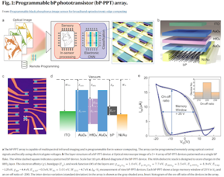
Abstract: Image sensors with internal computing capability enable in-sensor computing that can significantly reduce the communication latency and power consumption for machine vision in distributed systems and robotics. Two-dimensional semiconductors have many advantages in realizing such intelligent vision sensors because of their tunable electrical and optical properties and amenability for heterogeneous integration. Here, we report a multifunctional infrared image sensor based on an array of black phosphorous programmable phototransistors (bP-PPT). By controlling the stored charges in the gate dielectric layers electrically and optically, the bP-PPT’s electrical conductance and photoresponsivity can be locally or remotely programmed with 5-bit precision to implement an in-sensor convolutional neural network (CNN). The sensor array can receive optical images transmitted over a broad spectral range in the infrared and perform inference computation to process and recognize the images with 92% accuracy. The demonstrated bP image sensor array can be scaled up to build a more complex vision-sensory neural network, which will find many promising applications for distributed and remote multispectral sensing.


It is now peer reviewed and officially published as an open access paper: https://www.nature.com/articles/s41467-022-29171-1

Peer review report and authors' responses are also publicly available. In particular, it is interesting to see the response to some comments and about pixel non-uniformities, material stability during etching and longevity of the sensor prototype. 

Some lightly edited excerpts from the reviews and authors responses below:

Reviewer: The optical image of the exfoliated flake clearly shows regions of varying thickness. How did the authors ensure each pixel is of the same thickness? 

Authors: The mechanically exfoliated bP has several regions with different thicknesses. We fabricated all the pixels within a large region with uniform optical contrast, as outlined by the red dotted line, indicating uniform thickness. The thickness of the region is also confirmed with atomic force microscopy.

Reviewer: There is hardly any characterisation data provided for the material. How much of it is oxidised?

Authors: The oxidation of bP, it is indeed a concern. To mitigate that, we exfoliated and transferred bP in an Ar-filled glovebox. The device was immediately loaded into the atomic layer deposition (ALD) chamber to deposit the Al2O3 / HfO2 /Al2O3 (AHA) multilayers, which encapsulate the bP flake to prevent oxidation and degradation. This has been a practice reported in the literature, which generally leads to oxidation of only a few layers. Thanks to the 35 nm thick AHA encapsulation layer, our device shows long-term stability with persistent electrical and optical properties for more than 3 months after fabrication. We discuss that in the response to question 7. Furthermore, Raman spectroscopy shows no sign of Px Oy or Hx POy forming during the fabrication process. Thus, we expect that the oxidation of bP flake is no more than 3 layers (or 1.5 nm), which, if any, marginally affects the optical and electrical properties of the bP-PPT device. 

Reviewer: Why did the authors focus only on the IR range when the black phosphorus can be even more broadband into the visible at the thickness used here?

Authors: The photoresponsivity of black phosphorus certainly extends to the visible band. We have
utilized both the visible and the IR range by engineering the device with the AHA stack: IR light to input images for optoelectronic in-sensor computing; visible light to optically program the device by activating the trapped charges and process the encoded images such as pattern recognition.

Reviewer: How long do the devices keep working in a stable manner?

Authors: We agree with the reviewer that more lifetime measurement data is important to ensure the
stability of the device’s operation. We have evaluated the performance of the bP-PPT devices over a long period of time (up to 3 months) ... the gate modulation, memory window, on-off ratio, and retention time of our devices remain consistent even 3 months after they were fabricated.

In today's day and age of Twitter, it's refreshing to see how science really progresses behind the scenes --- reviewers raising genuine concerns about a new technique; authors graciously accepting limitations and suggesting improvements and alternative ways forward.

[Updated] 2022 International SPAD Sensor Workshop Final Program Available

About ISSW 2022

Devices | Architectures | Applications

The International SPAD Sensor Workshop focuses on the study, modeling, design, fabrication, and characterization of SPAD sensors. The workshop welcomes all researchers, practitioners, and educators interested in SPADs, SPAD imagers, and associated applications, not only in imaging but also in other fields.

The third edition of the workshop will gather experts in all areas of SPADs and SPAD related applications using Internet virtual conference technology.  The program is under development, expect three full days of with over 40 speakers from all over the world. This edition is sponsored by ams OSRAM.

Workshop website: https://issw2022.at/

Final program: https://issw2022.at/wp-content/uploads/2022/03/amsOSRAM_ISSW22_Program_3003.pdf


Tuesday, March 29, 2022

Hamamatsu Develops World's First THz Image Intensifier

Hamamatsu Photonics has developed the world’s first terahertz image intensifier (THz image intensifier or simply THz-I.I.) by leveraging its imaging technology fostered over many years. This THz-I.I. has high resolution and fast response which allows for real-time imaging of terahertz wave (*) pulses transmitted through or reflected from target objects.

This THz-I.I. will be unveiled at “The 69th JSAP (Japan Society of Applied Physics) Spring Meeting” held at the Sagamihara Campus of Aoyama Gakuin University (in Sagamihara City, Kanagawa Prefecture, Japan) for 5 days from Tuesday, March 22 to Saturday, March 26.
 

Terahertz waves are electromagnetic waves near a frequency of 1 THz and have the properties of both light and radio waves.


 Full press release: https://www.hamamatsu.com/content/dam/hamamatsu-photonics/sites/documents/01_HQ/01_news/01_news_2022/2022_03_14_en.pdf

Monday, March 28, 2022

Lensless camera for in vivo microscopy

A team comprised of researchers from Rice University and Baylor College of Medicine in Houston, TX has published a Nature Biomedical Engineering article titled "In vivo lensless microscopy via a phase mask generating diffraction patterns with high-contrast contours."

Abstract: The simple and compact optics of lensless microscopes and the associated computational algorithms allow for large fields of view and the refocusing of the captured images. However, existing lensless techniques cannot accurately reconstruct the typical low-contrast images of optically dense biological tissue. Here we show that lensless imaging of tissue in vivo can be achieved via an optical phase mask designed to create a point spread function consisting of high-contrast contours with a broad spectrum of spatial frequencies. We built a prototype lensless microscope incorporating the ‘contour’ phase mask and used it to image calcium dynamics in the cortex of live mice (over a field of view of about 16 mm2) and in freely moving Hydra vulgaris, as well as microvasculature in the oral mucosa of volunteers. The low cost, small form factor and computational refocusing capability of in vivo lensless microscopy may open it up to clinical uses, especially for imaging difficult-to-reach areas of the body.


Link to full article (open access): https://www.nature.com/articles/s41551-022-00851-z

Press release: https://www.photonics.com/Articles/Lensless_Camera_Captures_Cellular-Level_3D_Details/a67869

Sunday, March 27, 2022

Lensless Imaging with Fresnel Zone Plates

Although the idea of Fresnel zone plates is not new and can be traced back several decades to X-ray imaging and perhaps to Fresnel's original paper from 1818*, there is renewed interest in this idea for visible light imaging due to the need for compact form-factor cameras.

This 2020 article in the journal Light: Science and Applications by a team from Tsinghua University and MIT describes a lensless image sensor with a compressed-sensing style inverse reconstruction algorithm for high resolution color imaging.

Lensless imaging eliminates the need for geometric isomorphism between a scene and an image while allowing the construction of compact, lightweight imaging systems. However, a challenging inverse problem remains due to the low reconstructed signal-to-noise ratio. Current implementations require multiple masks or multiple shots to denoise the reconstruction. We propose single-shot lensless imaging with a Fresnel zone aperture and incoherent illumination. By using the Fresnel zone aperture to encode the incoherent rays in wavefront-like form, the captured pattern has the same form as the inline hologram. Since conventional backpropagation reconstruction is troubled by the twin-image problem, we show that the compressive sensing algorithm is effective in removing this twin-image artifact due to the sparsity in natural scenes. The reconstruction with a significantly improved signal-to-noise ratio from a single-shot image promotes a camera architecture that is flat and reliable in its structure and free of the need for strict calibration.


Full article is available here: https://www.nature.com/articles/s41377-020-0289-9

* "Calcul de l'intensité de la lumière au centre de l'ombre d'un ecran et d'une ouverture circulaires eclairés par un point radieux," in Œuvres Complètes d'Augustin Fresnel 1866-1870. https://gallica.bnf.fr/ark:/12148/bpt6k1512245j/f917.item

Friday, March 25, 2022

State of the Image Sensor Market

Sigmaintell report on smartphone image sensors

According to Sigmaintell, the global mobile phone image sensor shipments in 2021 will be approximately 5.37B units, a YoY decrease of about 11.8%; among which, the global mobile phone image sensor shipments in 4Q21 will be about 1.37B units, a YoY decrease. About 25.3%. At the same time, it is estimated that the global mobile phone image sensor shipments will be about 5.50B in 2022, a year-on-year increase of about 2.5%. In 1H21, due to the long ramp-up cycle of ultra-high pixel production capacity and the squeeze of low-end pixel production capacity by other applications, there was a short-term structural imbalance and market price fluctuations rose. In 2H21, the production capacity of Samsung and Sony’s external foundries was released steadily and significantly, but the sales in the terminal market were lower than expected and the stocking plan was lowered again, resulting in an oversupply in the overall image sensor market.


Business Korea report about Samsung CIS foundry capacity expansion


Samsung Electronics will expand its foundry capacity in legacy nodes starting in 2022. The move is aimed at securing new customers and boosting profitability by increasing the production capacity of mature processes for such items as CMOS image sensors (CISs), which are in growing demand due to a prolonged shortage. At the same time, Samsung Electronics is planning to start volume production of advanced chips on its sub-3nm fabrication process in 1H22. Samsung Electronics plans to secure up to 300 foundry customers by 2026 and triple production from the 2017 level. (Laoyaoba, Business Korea)


Yole announces a new edition of its "Imaging for Security" Market report

https://www.i-micronews.com/products/imaging-for-security-2022


Yole announces a new edition of its "Imaging for Automotive" market report

Flyer: https://s3.i-micronews.com/uploads/2022/03/YINTR22245-Imaging-for-Automotive-2022-Product-Brochure.pdf


Strategy Analytics estimates USD15.1B global smartphone image sensor market in 2021

According to Strategy Analytics, the global smartphone Image sensor market in 2021 secured a total revenue of USD15.1B. Strategy Analytics finds that the smartphone image sensor market witnessed a revenue growth of more than 3% YoY in 2021. Sony Semiconductor Solutions topped with 45% revenue share followed by Samsung System LSI and OmniVision in 2021. The top 3 vendors captured nearly 83% revenue share in the global smartphone image sensor market in 2021. In terms of smartphone multi-camera application, Image sensors for Depth and Macro application reached 30 percent share while those for Ultrawide application exceeded 15% share.


ijiwei Insights predicts drop in mobile phone camera prices

In 2022, some manufacturers will reportedly reduce the price of mobile phone camera CIS several times. Currently, the cost down of phone camera CIS has penetrated into the camera chip products of 2MP, 5MP and 8MP. Among them, the unit price of 2MP and 5MP mobile phone camera CIS fell by about 20% and more than 30% year-on-year, respectively. [source]

New 3D Imaging Method for Microscopes

New method for high resolution three dimension microscopic imaging being explored.


"This method, named bijective illumination collection imaging (BICI), can extend the range of high-resolution imaging by over 12-fold compared to the state-of-the-art imaging techniques," says Pahlevani

Fig. 1 | BICI concept. 
a, The illumination beam is generated by collimated light positioned off the imaging optical axis. 
b, The metasurface bends a ray family (sheet) originating from an arc of radius r by a constant angle β to form a focal point on the z axis. A family of rays originating from the same arc is shown as a ray sheet. 
c, Ray sheets subject to the same bending model constitute a focal line along the z axis. The focal line is continuous even though a finite number of focal points is illustrated for clarity. 
d, The collection metasurface establishes trajectories of collected light in ray sheets, as mirror images of illumination paths with respect to the x–z plane. This configuration enables a one-to-one correspondence, that is, a bijective relation between the focal points of the illumination and collection paths, to eliminate out-of-focus signals. The magnified inset demonstrates the bijective relation. 
e, Top view of the illumination and collection beams. 
f, Schematic of the illumination and collection beams and a snapshot captured using a camera from one of the lateral planes intersecting the focal line, illustrating the actual arrangement of illumination and collection paths. This arrangement allows only the collection of photons originating from the corresponding illumination focal point.


Metasurface-based bijective illumination collection imaging provides high-resolution tomography in three dimensions (Masoud Pahlevaninezhad, Yao-Wei Huang , Majid Pahlevani , Brett Bouma, Melissa J. Suter , Federico Capasso  and Hamid Pahlevaninezhad )

Thursday, March 24, 2022

Photonics Spectra article about Gigajot's QIS Tech

The March 2022 edition of Photonics Spectra magazine has an interesting article titled "Photon-Counting CMOS Sensors: Extend Frontiers in Scientific Imaging" by Dakota Robledo, Ph.D., senior image sensor scientist at Gigajot Technology.

While CMOS imagers have evolved significantly since the 1960s, photon-counting sensitivity has still required the use of specialized sensors that often come with detrimental drawbacks. This changed recently with the emergence of new quanta image sensor (QIS) technology, which pushes CMOS imaging capabilities to their fundamental limit while also delivering high-resolution, high-speed, and low-power linear photon counting at room temperature. First proposed in 2005 by Eric Fossum, who pioneered the CMOS imaging sensor, the QIS paradigm envisioned a large array of specialized pixels, called jots, that are able to accurately detect single photons at a very fast frame rate . The technology’s unique combination of high resolution, high sensitivity, and high frame rate enables imaging capabilities that were previously impossible to achieve. The concept was also expanded further to include multibit QIS, wherein the jots can reliably enumerate more than a single photon. As a result, quanta image sensors can be used in higher light scenarios, versus other single-photon detectors, without saturating the pixels. The multibit QIS concept has already resulted in new sensor architectures using photon number resolution, with sufficient photon capacity for high-dynamic-range imaging, and the ability to achieve competitive frame rates.


The article uses "bit-error-rate" metric for assessing image sensor quality.


The photon-counting error rate of a detector is often quantified by the bit error rate. The broadening of signals associated with various photo charge numbers causes the peaks and valleys in the overall distribution to become less distinct, and eventually to be indistinguishable. The bit error rate measures the fraction of false positive and false negative photon counts compared to the total photon count in each signal bin. Figure 4 shows the predicted bit error rate of a detector as a function of the read noise, which demonstrates the rapid rate reduction that occurs for very low-noise sensors. 


The article ends with a qualitative comparison between three popular single-photon image sensor technologies.


Interestingly, SPADs are listed as "No Photon Number Resolution" and "Low Manufacturability". It may be worth referring to previous blog posts for different perspectives on this issue. [1] [2] [3]

Full article available here: https://www.photonicsspectra-digital.com/photonicsspectra/march_2022/MobilePagedReplica.action?pm=1&folio=50#pg50


Wednesday, March 23, 2022

Axcelis to ship its processing tool to multiple CMOS image sensor manufacturers

BEVERLY, Mass., March 17, 2022 /PRNewswire/ -- Axcelis Technologies, Inc. (Nasdaq: ACLS), a leading supplier of innovative, high-productivity solutions for the semiconductor industry, announced today that it has shipped multiple Purion VXE™ high energy systems to multiple leading CMOS image sensor manufacturers located in Asia. The Purion VXE is an extended energy range solution for the industry leading Purion XE™ high energy implanter.

President and CEO Mary Puma commented, "We continue to maintain a leading position in the image sensor market. Our growth in this segment is clear and sustainable, and is tied to long-term trends in demand for products in the growing IoT, mobile and automotive markets. The Purion VXE was designed to address the specific needs of customers developing and manufacturing the most advanced CMOS image sensors, and has quickly become the process tool of record for image sensor manufacturers."

Source: https://www.prnewswire.com/news-releases/axcelis-announces-multiple-shipments-of-purion-high-energy-system-to-multiple-cmos-image-sensor-manufacturers-301504815.html

Tuesday, March 22, 2022

CMOS SPAD SoC for Fluorescence Imaging

Hot off the press! An article titled "A High Dynamic Range 128 x 120 3-D Stacked CMOS SPAD Image Sensor SoC for Fluorescence Microendoscopy" from the research group at The University of Edinburgh and STMicroelectronics is now available for early access in the IEEE Journal of Solid-State Circuits.

A miniaturized 1.4 mm x 1.4 mm, 128 x 120 single-photon avalanche diode (SPAD) image sensor with a five-wire interface is designed for time-resolved fluorescence microendoscopy. This is the first endoscopic chip-on-tip sensor capable of fluorescence lifetime imaging microscopy (FLIM). The sensor provides a novel, compact means to extend the photon counting dynamic range (DR) by partitioning the required bit depth between in-pixel counters and off-pixel noiseless frame summation. The sensor is implemented in STMicroelectronics 40-/90-nm 3-D-stacked backside-illuminated (BSI) CMOS process with 8-μm pixels and 45% fill factor. The sensor capabilities are demonstrated through FLIM examples, including ex vivo human lung tissue, obtained at video rate.


Full article is available here: https://ieeexplore.ieee.org/document/9723499 

Open access version: https://www.pure.ed.ac.uk/ws/portalfiles/portal/252858429/JSSC_acceptedFeb2022.pdf

Monday, March 21, 2022

Future Era of Robotics and Metaverse

SK hynix discusses what a robotic future may look like and the role of ToF imaging.

"We will soon witness an era where all households will have at least one robot that looks like it appeared in the scenes of a sci-fi movie like Star Wars."

Image Sensors Europe - Event Agenda Announcement

The Image Sensor  Europe team announced details about the upcoming event.

 2022 Event Topics Include (agenda link):

    Topic Speaker
    IMAGE SENSOR MANUFACTURING TRENDS AND BUSINESS UPDATES Markus Cappellaro
    Emerging from the global semiconductor shortage, what is the near-term outlook of the CIS industry? Florian Domengie
    Sony's contribution to the smarter industry - technology trends and future prospects for imaging and sensing devices Amos Fenigstein Ph.D.
    Panel discussion: how is the IS supply chain responding to sustainability and the green agenda?
    TECHNOLOGY FUTURES – LOOKING OUTSIDE THE BOX Anders Johannesson
    Efficiently detecting photon energy. The spin out from astronomy to industry has been paradigm shifting in the past – will this happen again? Kieran O'Brien
    Angular dependency of light sensitivity and parasitic light sensitivity Albert Theuwissen
    Augmented reality – the next frontier of image sensors and compute systems Dr Chiao Liu
    Sensing solutions for in cabin monitoring Tomas Geurts
    Global shutter sensors with single-exposure high dynamic range Dr. Guang Yang
    High resolution 4K HDR image sensors for security, VR/AR, automotive, and other emerging applications David Mills
    Bringing colour night vision and HDR image sensors to consumers and professionals Dr Saleh Masoodian
    Spectral sensing for mobile devices Jonathan Borremans
    Making infrared imaging more accessible with quantum dots Jiwon Lee
    Release 4 of the EMVA 1288 standard: adapted and extended to modern image sensors Prof. Dr. Bernd Jähne
    Design, characterisation and application of indirect time-of-flight sensor for machine vision Dr. Xinyang Wang
    Addressing the challenges in sustainability and security with low-power depth sensing Dr Sara Pellegrini, Cedric Tubert
    Establishing LiDAR standards for safe level 3 automated driving Oren Buskila
    Modelling and realisation of a SPAD-based LIDAR image sensor for space applications Alessandro Tontini
    Low-power Always-on Camera (AoC) architecture with AP-centric clock and 2-way communications Soo-Yong Kim
    Resolution of cinesensors: why higher resolution does not always improve image quality Michael Cieslinsk
    Latest developments in high-speed imaging for industrial and scientific applications Jeroen Hoet
    Event-based sensors – from promise to products Luca Verre
    Development of OPD innovative application, such as fingerprint behind display or standalone biometry solutions Camille Dupoiron
    Medical applications roundtable Renato Turchetta


Sony standardization efforts

Sony presents its effort to make its proprietary image sensor interface SLVS-EC a new international standard. Here's an excerpt from a recently published interview with K. Koide, M. Akahide, and H. Takahashi of the Sony Semiconductor Solutions group.  

Koide:I work in the standardization for the mobility area. Products in this category, such as automobiles, are strictly regulated by laws and regulations because of their immediate implications to society, the natural environment, and economic activities as well as to people’s lives and assets. Therefore, products that fail to comply with these laws and regulations cannot even make it to the market. On top of the compliance as a prerequisite, safety must be ensured. This “safety” requires cooperation of diverse stakeholders, from those who are involved in car manufacturing, automotive components, and transport infrastructure such as road systems to road users and local residents. My responsibilities include identifying the rules to be established in order to ensure safety as well as considering the domains and technology relevant to the rules where SSS Group can make its contributions and preparing our business strategies ready for the implementation.

Takahashi:I am involved in the standardization concerning the telecommunication of mobile devices like smartphones and automotive mobility devices. The telecommunication requires the transmitter and the receiver of signals use the same language, and standardization is essential for this reason. The telecommunication subgroup is standardizing the protocol, process, and electronic signal concerning the communication between an image sensor and processor.

Akahide:Like Takahashi-san, I am working on the standardization of image sensor interfaces. This is intended for image sensors for industrial applications. I was invited to work with the Japan Industrial Imaging Association (JIIA) on standardization because they wanted to standardize our SLVS-EC, a high-speed interface which SSS Group developed. As mentioned earlier, interfaces would be worth very little if they were not adopted widely. I believe that this standardization is very important for us, too, so that our high-speed interface will be diffused. At the same time, it is also important to develop a strategy for the future success of the product by determining what to be made open and what should be kept closed.

Koide:The world is growing more complex, and the COVID-19 pandemic is causing more uncertainties. Against this backdrop, there are serious discussions in progress about digitizing road systems, realizing zero-emission vehicles, and so on. The mobility industry is now experiencing a major social paradigm shift. At times like these, what we have for solidarity is order and rules to attain a better world. It is very important to understand these order and rules without prejudice, and to do this, we must engage with the world outside our boundaries, observing and understanding the world from their point of view. I believe that the activities with the mobility industry, including the initiative for developing the international standards, are valuable for me in this sense. For I am engaged in activities for the mobility industry, providing society with safety and security should be my priority. I will therefore continue my best efforts in this standardization initiative while also contributing to the business growth of our company.

Takahashi:For me, it will be making appropriate rules. There is a well-known episode about the washing machines. In 2001, Singapore suspended importing Japanese top-loading washing machines with a spinning drum. The reason for this was that these products did not comply with the international standards. They surely complied with the Japanese industrial standards, but not the international standards, which were based on IEC standards for front-loading single-drum machines popular in Europe and America. Rules have the power to control. As a chair, I would like to pursue making rules that are appropriate and that do not work against SSS Group.
From a more specific viewpoint, there is the issue concerning image sensors. They are increasingly sophisticated that captured image data can be edited easily, boosting the added value of the sensors. However, there was a problematic incident. When a major earthquake hit Kumamoto, someone uploaded on social media a fake video footage of a lion set loose from the local zoo, which many people believed. Security will be important about camera information in the future, and it is necessary to be able to verify the authenticity of images. I hope that new standards will be established to help prevent fake images such as this from being circulated.

Akahide:Joining the SDO has made me realize that everyone has high hopes for SSS Group. My next step will be dedicated to the standardization of our technology and, also as a vice leader of the Global Standardization Advancement Committee, I should be making contributions to the machine vision sector.


The interview does not provide any technical information about SLVS-EC and how it differs from the MIPI M-PHY standard.

Full interview available here: https://www.sony-semicon.co.jp/e/feature/2022031801.html

Weekly Updates


Nikon Designs Sensor That Has Both a Global and Rolling Shutter

Nikon has filed a patent for a new type of sensor that would allow it to perform both a rolling and global shutter operation. It’s not the first time the company has proposed such a design, but it expands on the use case of a previous filing. ...


Programmable Black Phosphorus Image Sensor For Broadband Optoelectronic Edge Computing

Image sensors with internal computing capability enable in-sensor computing that can significantly reduce the communication latency and power consumption for machine vision in distributed systems and robotics. Two-dimensional semiconductors have many advantages in realizing such intelligent vision sensors because of their tunable electrical and optical properties and amenability for heterogeneous integration. ...


Samsung Quietly Unveils The Galaxy A73 5G, Its First Mid-Range Phone with a 108MP Camera


In 2020, Samsung introduced the Galaxy S20 Ultra to the market, and its main selling point was an all-new 108MP rear sensor. The camera experience was a little rough around the edges, but it improved a bit in the Note20 Ultra and the S21 Ultra and even more in this year's S22 Ultra. Up to this point, those 108MP cameras had remained a selling point of the Ultra range, as other S devices didn't get them. But now Samsung has unveiled the Galaxy A73 5G, the phone that's breaking that trend for the first time. ...


Intel Investing $100 Million in Semiconductor Education

"Our goal is to bring these programs and opportunities to a variety of two-year and four-year colleges, universities, and technical programs, because it is critical that we expand and diversify STEM education." An additional $50 million will be matched by the U.S. National Science Foundation (NSF), which will be asking for proposals from educators for a curriculum that aims to improve STEM education at two-year colleges and four-year universities. ...


The Neon Shortage Is a Bad Sign: Russia's war against Ukraine has ramifications for the chips that power all sorts of tech

Neon, a colorless and odorless gas, is typically not as exciting as it sounds, but this unassuming molecule happens to play a critical role in making the tech we use every day. For years, this neon has also mostly come from Ukraine, where just two companies purify enough to produce devices for much of the world, usually with little issue. At least, they did until Russia invaded. ...


Patent Tip, Based on a True Story: Contour IP Holdings, LLC v. GoPro

"Patent Owners should avoid describing and claiming the advance over the prior art in purely functional terms, in a result-oriented way that amounts to encompassing the abstract solution no matter how implemented. Instead, Patent Owners should describe and claim technical details for tangible components in the claimed system, showing that such components are technologically innovative and not generic. For computer-implemented inventions, this may include a specific set of computer digital structures to solve a specific computer problem." ...

Thursday, March 17, 2022

In the News: Week of March 14, 2022

China COVID spike may affect image sensor supply

Digitimes Asia reports: "A spike in COVID-19 cases in Hong Kong and other Chinese cities is disrupting handset CMOS image sensor (CIS) shipments, as well as deliveries of related modules and other devices, according to industry sources." [source]


Luminous Computing Appoints Michael Hochberg as President

EETimes reports: "Luminous Computing, a machine learning systems company based in California, announced today the appointment of Michael Hochberg as president. Hochberg will lead engineering and operations at Luminous to develop what the company claims is the world’s most powerful artificial intelligence (AI) supercomputer to market, driven by silicon photonics technology. [source]


James Webb Telescope Camera Outperforming Expectations  

NASA reports: "On March 11, the Webb team completed the stage of alignment known as “fine phasing.” At this key stage in the commissioning of Webb’s Optical Telescope Element, every optical parameter that has been checked and tested is performing at, or above, expectations. The team also found no critical issues and no measurable contamination or blockages to Webb’s optical path. The observatory is able to successfully gather light from distant objects and deliver it to its instruments without issue." [source]

DSLR Confusion

Poking fun at a recent NYPost shopping guide on "Best DSLRs" list that contains mirrorless cameras, PetaPixel reports: "People Have No Idea What a DSLR Actually Is" [source] 

If you have any interesting news articles and other tidbits worth sharing on this blog please email ingle dot atul at ieee dot org.

Image Sensing via Photoacoustic Effect

A new preprint titled "An image sensor based on single-pulse photoacoustic electromagnetic detection (SPEED): a simulation study" proposes a concept image sensors that relies on the conversion of electromagnetic energy into sound (photoacoustic effect). The claim is that this technique can detect radiation over a much broader range of the electromagnetic spectrum.

Image sensors are the backbone of many imaging technologies of great importance to modern sciences, being particularly relevant in biomedicine. An ideal image sensor should be usable through all the electromagnetic spectrum (large bandwidth), it should be fast (millions of frames per second) to fulfil the needs of many microscopy applications, and it should be cheap, in order to ensure the sustainability of the healthcare system. However, current image sensor technologies have fundamental limitations in terms of bandwidth, imaging rate or price. In here, we briefly sketch the principles of an alternative image sensor concept termed Single-pulse Photoacoustic Electromagnetic Detection (SPEED). SPEED leverages the principles of optoacoustic (photoacoustic) tomography to overcome several of the hard limitations of todays image sensors. Specifically, SPEED sensors can operate with a massive portion of the electromagnetic spectrum at high frame rate (millions of frames per second) and low cost. Using simulations, we demonstrate the feasibility of the SPEED methodology and we discuss the step towards its implementation.


[Blog poster's comments: I think this is an interesting concept, especially given that there are ultrasonic transducers based on CMUT (capacitive micromachined ultrasound tranducer) technology which can be miniaturized and manufactured at scale using a CMUT-in-CMOS process. For example, the Butterfly iQ handheld ultrasound scanner has 9000 CMUT "pixels". However, overall spatial resolution will still be a challenge with current technology. The 1/20x simulation shown in this preprint (see bottom figure above) is still an optimistic case.]