Saturday, October 31, 2020

Hynix Unveils its First ToF Sensor

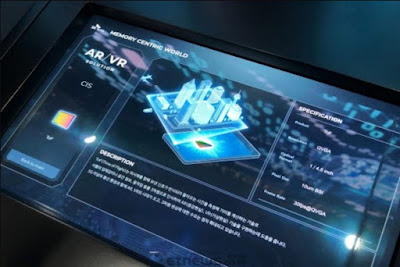
Korea IT News: SK Hynix introduces its TOF image sensor at “SEDEX 2020” exhibition this week. Its sensor has 10µm BSI pixels and QVGA resolution in 1/4.5-inch format. The sensor is still in development and its release date has not been disclosed.

SK Hynix TOF sensor is a part of its plan to grow its image sensor business. The company opened a R&D center in Japan last year that primarily focuses on image sensor technology. It also reorganized its lineup of image sensors for smartphone cameras this year. It supplies sensors with increased pixel numbers and smaller pixel size to major smartphone manufacturers. It is currently working on sensors with high pixel numbers such as 48MP and 64MP sensors.

Friday, October 30, 2020

SK Hynix: The Latest Technology Trend in CIS is about Functions, not Pixel

 SK Hynix Head of CIS ISP Taehyun (Ted) Kim publishes a post "The Visual Evolution & Innovation of Image Sensors." Few quotes:

"...this trend for high pixels in CIS is expected to face technical difficulties soon, and the innovation for a high level of functions centered on the ISP will be in full swing.

This is due to the limits of miniaturization of CIS pixels due to the diffraction limit. It is possible to reduce the critical dimension of electric circuits to several nanometers with the current semiconductor technology; however, since the light reception amount decreases as the pixel size decreases, the sensitivity and the signal level is reduced, resulting in the decline in SNR and the image quality degradation.

Currently, SK hynix’s CIS has built-in image processing functions such as phase detection auto focus (PDAF), Quad pixel processing, and high dynamic range (HDR) processing, and new functions are constantly being added to it.

Currently, SK hynix’s CIS, mainly the Black Pearl product line, is widely used in smartphone cameras and the application field is expected to expand to various fields such as bio, security, and autonomous vehicles.

In the future, CIS is expected to evolve into an information sensor that supports advanced additional functions, without being limited to image quality improvement. SK hynix’s stack sensor is already capable of embedding a simple AI hardware engine inside the ISP on the lower substrate, based on the advanced semiconductor process. Based on this, SK hynix is currently developing new machine learning-based technologies such as super resolution, color restoration, face recognition, and object recognition."

Fujifilm Uses Polarization Sensor for Multispectral Imaging

OSA Optics Express paper "Snapshot multispectral imaging using a pixel-wise polarization color image sensor" by Shuji Ono, Fujifilm, uses polarization to separate multispectral filter bands:

"This study proposes a new imaging technique for snapshot multispectral imaging in which a multispectral image was captured using an imaging lens that combines a set of multiple spectral filters and polarization filters, as well as a pixel-wise color polarization image sensor. The author produced a prototype nine-band multispectral camera system that covered from visible to near-infrared regions and was very compact. The camera’s spectral performance was evaluated using experiments; moreover, the camera was used to detect the freshness of food and the activity of wild plants and was mounted on a vehicle to obtain a multispectral video while driving."

One More HDR Pixel Paper

Sensing and Imaging An International Journal publishes a paper "On Wide Dynamic Range Tone Mapping CMOS Image Sensor" by Waqas Mughal and Bhaskar Choubey from University of Southampton, UK, and Universitat Siegen, Germany.

"The dynamic range of a natural scene often covers over 6 decades of intensity from bright to dark areas. Typical image sensors, however, have limited ability to capture this dynamic range available in nature. Even after designing specific wide dynamic range (WDR) image sensors, displaying them on conventional media with limited ability requires computationally complex tone mapping. This paper proposed a novel CMOS pixel which can capture and perform tone mapping during data acquisition. The pixel requires a reference voltage to generate tone mapped response. A number of different reference signals are proposed and generated which can perform WDR operation. Nevertheless, fixed pattern noise (FPN) effects the performance of these pixel. A pixel model with simple parameter extraction procedure is described for a typical tone mapping operator. This model is then used to obtain a simple procedure for pixel calibration leading to reduced FPN. The new proposed pixel response is able to capture upto 6 decades of light intensity and reported FPN correction procedure produces 1% of FPN contrast error."

Thursday, October 29, 2020

Sony 33-Sensor Concept Car

NikkeiAsia: "I believe the next megatrend [after mobile phones] will be mobility," said Sony Chairman and President Kenichiro Yoshida as he unveiled the Vision-S concept car at the CES tech show in the U.S. in January.

The Vision-S will have 33 sensors, including image sensors, a Sony specialty. Izumi Kawanishi, Sony's SVP who is shepherding development of the car, said the sensors "give passengers and pedestrians a sense of security thanks to the 360-degree vision it provides."

NikkeiAsia says that Sony controls about 70% of the global market for the image sensors used in smartphone cameras, but its share for automotive image sensors is only 9%. The Vision-S is an exploratory effort by the company as it taps into a market led by ON Semi. According to NikkeiAsia, ON Semi has been producing automotive image sensors for over 50 years (since 1970?) and controls 45% of the market.

Sony and Omnivision Receive US License to Supply Sensors to Huawei

Nikkei reports that Sony and Omnivision have been granted licenses by the U.S. government to resume some shipments to China's Huawei.

"What we learned was that some... image sensor related suppliers are receiving some licenses from the U.S. government as those components are viewed as less related to cybersecurity concerns, and Sony is among those who received approval," an unnamed chip industry executive told Nikkei Asia.

Wednesday, October 28, 2020

Light Launches Clarity, Better than LiDAR

 Light Co. announces its automotive 3D depth Clarity platform:

"Lidars do a great job, but they don’t do the whole job. Their range is often limited to ~250 meters. Class 8 trucks need at least 400+ meters to come to a complete stop, safely. Lidar as well as monocular camera-based systems can get confused as to whether they’re seeing a person painted on the side of a truck or an actual person.

Clarity is a camera-based perception platform that’s able to see any 3D structures in the road from 10 centimeters to 1000 meters away — three times the distance of the best-in-class lidar with 20 times the detail."


There is nothing else like the Clarity platform with its combination of depth range, accuracy, and density per second. It enables a new generation of vehicles that can be made safer, without having to compromise on cost, quality, or reliability,” said Prashant Velagaleti, Chief Product Officer of Light. “Rather than only minimizing the severity of a collision, having high fidelity depth allows any vehicle powered by Clarity to make decisions that can avoid accidents, keeping occupants safe as well as comfortable.” 


Sony Reports 1% Decrease in Image Sensor Sales, Reduces Forecast

Sony reports its quarterly results and updates on its image sensor business:


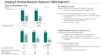
  • FY20 Q2 sales decreased slightly year-on-year to 307.1 billion yen and operating income significantly decreased 26.5 billion yen to 49.8 billion yen.
  • FY20 sales are expected to decrease 40 billion yen to 960 billion yen and operating income is expected to significantly decrease 49 billion yen to 81 billion yen.
  • Even accounting for the decrease in operating income in FY20, we expect the difference between the total of operating cash flow and investing cash flow for the segment over the three fiscal years begun April 1, 2018 to be positive.
  • Pursuant to export restrictions announced by the U.S. government on August 17, 2020 we terminated product shipments to a certain major Chinese customer [Huawei - ISW] as of September 15, 2020.
  • The forecast disclosed today for the second half of this fiscal year does not include any shipments to that customer.
  • In addition, the operating income for the quarter includes an approximately 17.5 billion yen write-down of finished goods and work-in-progress inventory for that customer recorded at the end of September.
  • Based on this situation, we are further revising the business strategy, as I explained at the previous earnings announcement, from the perspective of capital expenditures, research and development and customer base.
  • We are further postponing the timing of capital expenditures, with cumulative capital expenditures for the three fiscal years begun April 1, 2018 expected to be reduced 40 billion yen from the approximately 650 billion yen I explained last time.
  • We do not think it is prudent to prematurely reduce research and development spending because we want to meet the needs of a wide range of smartphone customers, as well as maintain and increase our future technological competitive advantage.
  • We have had some success expanding and diversifying our customer base for FY21. The financial impact on our business in FY20 is limited, but we think it is possible to recapture, in FY21, a large portion of the market share, on a unit basis, we lost this fiscal year.
  • However, we expect that it will take a long time for other customers to follow the trend to higher-functionality and larger die-sized smartphone cameras that the Chinese customer [Huawei - ISW] was leading. Thus, we expect the substantial recovery of profitability driven by these high value-added products to take place in the fiscal year ending March 31, 2023 (“FY22”).
  • By recapturing market share in FY21 through an increase in sales of commodity sensors, and by recouping our business profitability in FY22 through more high valueadded products, we aim to return the mobile image sensor business to growth.
  • In addition, there is no change to our mid-to long-term strategy of growing our business through expansion of applications that use edge AI and 3D sensing capabilities, as well as through starting up automotive sensors in earnest.
Reuters reports that Huawei was Sony’s second-largest image sensor customer after Apple, accounting for about 20% of its $10b in sensor revenue, according to analyst estimates.

Will the iPhone LiDAR Change AR Forever?

 AWE publishes a panel discussion "AWE Nite NYC: Will the iPhone LiDAR Change AR Forever? With Snap, Niantic, Occipital."

Infineon and PMD Announce 10m Long Range ToF Sensor for Smartphones

BusinessWire: Infineon and pmdtechnologies developed a 3D ToF sensor which is claimed to outperform other solutions in the market and aims for a wider spectrum of consumer applications. The 3D sensor market in smartphones for rear side cameras is expected to grow up to more than 500M units per year until 2024.

The latest 3D image sensor from Infineon and pmdtechnologies enables a new generation of applications”, says Philipp von Schierstaedt, SVP Infineon. “It aims to create most immersive and smarter AR experiences as well as better photography results with a faster autofocus in low-light conditions or more beautiful night mode portraits based on picture segmentation. This latest chip development is truly setting standards when it comes to improvements of the imager, the driver and processing as well as unprecedented ten meters long range capabilities at lowest power.

The new chip allows the integration into miniaturized camera modules, accurately measuring depth in short and long range for AR while meeting low power consumption requirements with more than 40% power saving on the imager.

Furthermore seamless augmented reality sensing experiences are being achieved, allowing for high quality 3D depth data capture up to a distance of 10m (at reduced resolution), without losing resolution in the shorter range. Always-on applications such as mobile AR gaming can greatly benefit from the small power budget required by the new sensor. For applications such as the 3D scanning for room and object reconstruction or 3D mapping for furniture planning and other design applications the sensor allows to double the measuring range beyond the current solution in the market.

The volume delivery for this chip starts in Q2 2021, demo kits are already available. The recorded livestream from the official press event is available here: https://livestream.com/infineontechnologies/real3

Tuesday, October 27, 2020

ST Announces 64-Point dToF Sensor

GlobeNewswireSTMicroelectronics extends its portfolio of FlightSense ToF sensors with a 64-zone device. This first-of-its-kind product comprises a 940nm VCSEL light source, a SoC sensor integrating a VCSEL driver, the receiving array of SPADs, and a low-power 32-bit MCU core and accelerator running firmware. The VL53L5 retains the Class 1 certification of all ST’s FlightSense sensors and is fully eye-safe for consumer products.

The multi-zone VL53L5 FlightSense direct Time-of-Flight sensor uses our most advanced 40nm SPAD production process to offer outstanding 4m ranging performance and up to 64 ranging zones that help an imaging system build a detailed spatial understanding of the scene,” said Eric Aussedat, GM of ST’s Imaging Division. “Delivering 64x more ranging zones than previously available, the VL53L5 offers radical performance improvement in laser autofocus, touch-to-focus, presence detection, and gesture interfaces while helping developers create even more innovative imaging applications.

With a vertically integrated manufacturing model for its FlightSense sensors, ST builds its SPAD wafers on a 40nm proprietary silicon process in the Company’s 12” wafer plant at Crolles, France before assembling all of the module components in ST’s back-end plants in Asia. This approach delivers exceptional quality and reliability to customers.

Packaged in a 6.4 x 3.0 x 1.5 mm module, the VL53L5 integrates both transmit and receive lenses into the module design and expands the FoV of the module to 61-degrees diagonal. This wide FoV is especially suited to detect off-center objects and ensure perfect autofocus in the corners of the image. In the ‘Laser Autofocus’ use case, the VL53L5 gathers ranging data from up-to 64 zones across the full FoV to support “Touch to Focus” and many other features.

Further flexibility is available via the SPAD array, which can be set to favor spatial resolution, where it outputs all 64 zones at up to 15fps, or to favor maximum ranging distance, where the sensor outputs 4×4/16 zones at a frame rate of 60fps.

ST’s architecture can automatically calibrate each ranging zone and direct Time-of-Flight technology allows each zone to detect multiple targets and reject reflection from the cover-glass. 

Customer development with the VL53L5 can build on ST’s strong relationships with key smartphone and PC platform suppliers as ST has pre-integrated the sensor onto these platforms. The VL53L5 is in mass production with millions of units already shipped to leading wireless and computer manufacturers.
Axcelis 5-8MeV Implanters Adopted by Multiple CIS Companies

PRNewswire: Axcelis announces that it has shipped multiple Purion VXE (up to 8MeV) and Purion EXE (up to 5.3MeV) high energy systems to several leading CMOS image sensor manufacturers. The systems shipped in the third quarter. There is no word on adaption the highest energy Purion XEmax supportint up to 15MeV ion implantation.

EVP of Product Development, Bill Bintz, commented, "Axcelis has created a flexible, highly differentiated high energy product portfolio that is ideally suited to address the exact needs of customers manufacturing image sensors for applications requiring ultra-high energy implants with extremely precise and deep doping profiles."

Omnivision to Increase its Wafer Testing Capacity by 420,000 12-inch Wafers per Year

Rising Sun Mobile News reports that Will Semi, Omnivision's mother company, intends to issue 2.69 billion yuan (approx. $400M) of convertible corporate bonds to build a wafer testing and reconstruction facility in Shanghai for Omnivision.  After the project is completed and put into production, 420,000 additional 12-inch wafers will be tested per year.

After the construction is completed, Omnivision would test and reconstruct wafers and sub-assembly of high-MP imagers on its own. This is expected to reduce processing costs and improve products more comprehensively. Also, it would reduce the proportion of the outsourced processing and associated supply chain risks.

Monday, October 26, 2020

Actlight Presents its Single Photon DPD for dToF Imaging

PRNewswireActlight presents its DPD with tunable sensitivity for direct ToF applications:


Sony R&D Stories

 Sony publishes an article "Sony’s Latest Image Sensors and the Technologies that Lies Behind Them." Few quotes:

"There are various types of ToF, and we focused on developing an indirect-ToF (iToF) method that works by measuring the phase delay of returning light after it has been reflected by the target object. To realize this sensor, we developed a new back-illuminated CAPD (Current Assisted Photonic Demodulator) by combining CAPD technology, which is an IP of Sony Depthsensing Solutions, with Sony’s back-illuminated CMOS image sensor technology.

Making the most of the back-illuminated structure, it efficiently converts light into electrons, enabling time detection of under 50 picoseconds and greatly improving distance resolution."


"Sony Depthsensing Solutions was an emerging company at that time and only a small number of skillful members were involved in the development. Right after we started collaborating, the difference in corporate cultures perplexed us. By making Sony Semiconductor Solutions’ team small too, requiring each member to be more responsible, we were able to realize rapid development while absorbing this unfamiliar culture. During the development, issues that we had never experienced before cropped up, including chips breaking while under evaluation, but we worked with each other and brought them to completion. In addition to image sensors, this collaboration between the two companies from Belgium and Japan also contributed to securing the iToF businesses."

"In the automotive industry, there are many international standards related to the product development process, which itself must also be refined along with the product in line with industry-wide standards. Using the evidence gathered during development, the validity of the process is demonstrated with the aim of establishing a firm position as a reliable supplier in the industry while being assessed and audited by customers. At first, we did not understand anything about the differences when compared with electronics products and the unique culture of the automotive industry, but we learned by reading standards and attending seminars, all the while striving to improve. In particular, it took a lot of time and effort to think about how to apply ideas defined on the vehicle level to the image sensor level."


"A unique technology called "SenSWIR" connects these different semiconductors via a Cu-Cu direct bonding, realizing the Sony’s innovative SWIR image sensor. By thinning the indium phosphide (InP) substrate that blocks visible light, the SWIR image sensor is able to capture a broad range of wavelengths, from visible to short-wave infrared, with high sensitivity."

Sunday, October 25, 2020

Cambridge Mechatronics to Unveil its 3D Camera Module Soon

Cambridge Mechatronics (CML) is preparing its own 3D camera module with 10m depth range:

"Apple’s technology is different to that used previously by other smartphone brands. The LiDAR module collects data from around six hundred points of emitted light. In addition to images from other cameras in the handset, this information is processed by the neural engine in the iPhone to simulate detailed depth data of the scene up to five metres away.

CML has also been working on long range 3D sensing. Using our patented technology, we have developed a module that collects three hundred thousand data points at a range of ten metres. No supporting information is required from other cameras to deliver the 3D experience. The high resolution of the depth map in CML’s solution removes the necessity to pass it through a neural engine, making it a simple solution to include in smartphones and other products.

By extending range from five to ten metres, augmented reality can be applied to more of the surroundings, opening up an even greater number of applications and a more realistic, immersive experience. This gives even more freedom and opportunities for apps developers.

We will be promoting our 3D sensing modules to the market shortly."

poLight AF Reverse Engineering

SystemPlus publishes a reverse engineering report of poLight AF lens:

"This is a radical technology shift in the camera module world, thanks to the exceedingly small volume of the autofocus. It measures only 8.4mm3, and with a thickness of 0.45mm can be easily integrated in small systems like drones, smartphones, smart watches, etc. We discovered this autofocus in Xiaomi’s latest smartwatch for kids: the Mitu 4 Pro.

The assembly of this autofocus on an 8Mpixels camera module is detailed in our study. Thanks to the PZT, it is faster than the traditional electromechanical autofocus, allowing for almost instantaneous autofocus autofocus adjustment. And with no mechanical parts aside from the membrane, the MEMS autofocus seems more robust than mechanical systems, which is vital in products for children.

The piezoelectric membrane is manufactured by STMicroelectronics, which specifically developed PZT technology to add to its MEMS technology portfolio. Another specific MEMS process is the transducer, which is manufactured on glass membranes etched by micromachining – another specialty of STMicroelectronics.

The secret of this first MEMS autofocus is not only in the piezoelectric material. The design, manufacturing, and characteristics of the polymer used for the lens were developed and patented by poLight, and these things are key for the functionality of the autofocus component."

SeeDevice Updates its Comparisons

SeeDevice added few more comparisons of its Quantum Tunneling PAT-PD imager with CMOS sensors:

Saturday, October 24, 2020

Michael Tompsett and Bell Labs Receive Emmy Award for the First CCD Imager

Cape Cod Chronicle and Nokia Bell Labs report that The National Academy of Television Arts & Sciences 2020 technical Emmy award winners goes to imaging CCD inventors Michael Tompsett and Bell Labs. Tompsett's invention of CCD imager launched the digital imaging industry and was used in the first commercially available digital cameras.

Friday, October 23, 2020

Huawei Mate 40 Features Always-On Front Camera

Huawei announces its Mate 40 series smartphones with new camera features. The front camera implements an always-on vision-based user interface:

"HUAWEI Mate 40 Pro and HUAWEI Mate 40 Pro+ are set to revolutionise how consumers integrate smartphones into their lives with new user-centric features including Smart Gesture Control, which allows total hands-free control of your device. Simply hover your hand over the device to wake it up or navigate your phone by swiping left, right, up and down. There is also an air press gesture for call answering.

A device that is always there for you, the all new dynamic Eyes on Display on HUAWEI Mate 40 Pro and HUAWEI Mate 40 Pro+ can be activated at a glance, with fully customisable interactive displays hosting all the information you need from your phone. The ring of incoming calls can be reduced by making eye contact with your phone."

Here are official Huawei demos of its low-power vision camera:


Few other innovations in Mate 40 cameras: