Wednesday, June 30, 2021

Isorg Raises 16M Euros in Series C Round

ALA News: Isorg announces a capital increase of €16M in series C financing. Two major industrial investors, Sumitomo Chemical and Mitsubishi participated in the round. Greece-based Integrated Systems Development SA and five new French investors represented by fund manager Financière Fonds Privés also joined the round. Legacy shareholders Bpifrance, through its large venture funds, New Science Venture, CEA Investment and Sofimac Group (Limousin Participations) contributed, reaffirming their commitment and confidence in Isorg. The company has raised €47.8M (approx. $58.4M) to date.

This third fundraising marks Isorg’s maturity and readiness to become the industrial player we set out to be at the very start of our venture 11 years ago,” said Jean Yves Gomez, CEO of Isorg. “The addition of new industrial investors from Japan and Greece, alongside our historical partners, is confirmation of our international ambition, the strength of our business model and product maturity.

Isorg will use the new proceeds to:
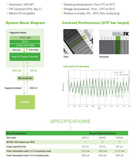
  • Launch the commercial availability of its organic photodiode technology to provide the security market with increased levels of ID authentication and offer new integration opportunities for multiple fingerprint scanners
  • Deploy a global sales and applications engineering workforce
  • Transform operations to support a fully-fledged industrial company
OPD technology can be used in a variety of applications. We expect the OPD market will soon boom and expand rapidly through Isorg’s technology,” said Isao Kurimoto, executive officer at Sumitomo Chemical Co Ltd.

Besides integration in smartphones, Isorg’s solutions can be applied in a wide range of applications for different industry domains,” declared Yoshiyuki Watanabe, general manager of the business creation & digital strategy unit at Mitsubishi Corporation.

Over the coming months, Isorg plans to achieve several goals:
  • Open a new location in Asia
  • File FBI certification for its FAP20 to FAP60 biometrics modules for security applications
  • Develop palm size modules
  • Design a vein recognition module based on a client-validated sensor with strong NIR sensitivity


Automotive PHY Battles: A-PHY vs Auto-Serdes, Sony Evaluates A-PHY

PRNewswire: Valens announces that it has started an evaluation with Sony Semiconductor Solutions to develop and integrate MIPI A-PHY technology into next-generation image sensor products.

A-PHY Serdes standard was released by the MIPI Alliance in September 2020 aiming for integration of cameras, sensors and displays in vehicles, while also incorporating functional safety and security. Valens is the first company to market with A-PHY compliant chipsets. Recently, Valens announces a PAC deal to list at NYSE at valuation of $1.16B. (EETimes)

"It's highly important for Sony to integrate the cutting-edge technology into our image sensors, and A-PHY serializer integration will provide significant benefits for our customers," said Kenji Onishi, General Manager, Automotive Business Department, Sony Semiconductor Solutions. "The MIPI ecosystem is growing quickly, and we're happy to be early adopters of this automotive connectivity standard. Valens is in a leading position with A-PHY, which is why it is so important for us to start this collaboration. We believe future models will have even higher resolutions. In addition, our company is preparing to integrate several features into their next-generation sensors, including metadata output, higher framerate, and wider bit depth – all of which will require an ultra-high-speed, long-reach connectivity solution such as MIPI A-PHY. We will continue to support not only A-PHY but also D-PHY, proprietary interfaces, and open-standard interfaces."


MIPI A-PHY standard faces a competition of Automotive SerDes Alliance (ASA) that offers quite similar performance and feature set. SemiEngineering discusses the two standards competition:

"The reason for the separate and independent ASA development isn’t publicly clear. In some of their statements and materials, it is positioned as the only standardized alternative to proprietary schemes, without acknowledging the existence of the MIPI/VESA solutions. And some say that, during the A-PHY definition process, the group split, with one side moving to create the new ASA group.

Some further digging revealed that the main concern seems to be that the A-PHY technology comes from one company, Valens, which contributed it to the standard. However, “MIPI A-PHY, like all MIPI specifications, is made available under royalty-free terms,” said [Peter Lefkin, managing director of the MIPI Alliance.]

Still, the issue for ASA members appears to be that only essential patents get a license. Valens has implemented this in a way that includes non-essential patents, and licensees don’t get access to those patents. A statement from the ASA steering committee noted, “There are examples where the solution of one supplier was successfully made a standard, but there are many examples where it did not work.”

The ASA folks are more interested in a process where multiple companies contribute technology without one company dominating. The ASA effort is licensed under FRAND (free or reasonable and non-discriminatory) licensing.

MIPI’s concern is there may be royalty uncertainty prior to acquiring a license. There apparently has been some history in the automotive realm of companies refusing to license essential patents. Regardless, it’s pretty clear that the A-PHY and the ASA PHY will compete head-to-head. How that competition resolves itself is not yet evident."

SPAD Imaging with No Pile-Up

Politecnico di Milano, Italy, publishes an open access paper in Review of Scientific Instruments "Toward ultra-fast time-correlated single-photon counting: A compact module to surpass the pile-up limit" by S. Farinaa,  G. Acconcia, I. Labanca,  M. Ghioni, and  I. Rech.

"Time-Correlated Single-Photon Counting (TCSPC) is an excellent technique used in a great variety of scientific experiments to acquire exceptionally fast and faint light signals. Above all, in Fluorescence Lifetime Imaging (FLIM), it is widely recognized as the gold standard to record sub-nanosecond transient phenomena with picosecond precision. Unfortunately, TCSPC has an intrinsic limitation: to avoid the so-called pile-up distortion, the experiments have been historically carried out, limiting the acquisition rate below 5% of the excitation frequency. In 2017, we demonstrated that such a limitation can be overcome if the detector dead time is exactly matched with the excitation period, thus paving the way to unprecedented speedup of FLIM measurements. In this paper, we present the first single-channel system that implements the novel proposed methodology to be used in modern TCSPC experimental setups. To achieve this goal, we designed a compact detection head, including a custom single-photon avalanche diode externally driven by a fully integrated Active Quenching Circuit (AQC), featuring a finely tunable dead time and a short reset time. The output timing signal is extracted by using a picosecond precision Pick-Up Circuit (PUC) and fed to a newly developed timing module consisting of a mixed-architecture Fast Time to Amplitude Converter (F-TAC) followed by high-performance Analog-to-Digital Converters (ADCs). Data are transmitted in real-time to a Personal Computer (PC) at USB 3.0 rate for specific and custom elaboration. Preliminary experimental results show that the new TCSPC system is suitable for implementing the proposed technique, achieving, indeed, high timing precision along with a count rate as high as 40 Mcps."

Tuesday, June 29, 2021

Omnivision Unveils Disposable 8MP Sensor, More

BusinessWire: OmniVision announces its next-generation OH08A and OH08B CMOS sensors―the first 8MP sensors for single-use and reusable endoscopes. Additionally, the new OH08B is the first medical-grade image sensor to use Nyxel NIR technology.

The medical-grade OH08A image sensor features a 1/2.5-inch optical format, incorporates 1.4µm PureCel Plus-S pixel and offers 4K2K resolution in a small 7.1 x 4.6mm package for chip-on-tip endoscopes. The OH08B has a 1/1.8-inch optical format, uses a larger 2.0µm PureCel pixel in a 8.9 x 6.3mm package and features OmniVision’s Nyxel technology with enhanced NIR sensitivity.

Our next-generation OH08A/B 8MP image sensors are targeted at endoscopes with a 10-12mm outer diameter, such as gastroscopes, duodenoscopes, amnioscopes, laparoscopes and colonoscopes. They deliver higher image quality, up to 4K2K resolution at 60 fps, greatly improving the doctor’s ability to visualize the human anatomy during these important procedures,” said Richard Yang, senior staff product marketing manager at OmniVision. “In the OH08B, we’ve taken our sensor to the next level by adding Nyxel technology, which offers better performance in color and IR sensitivity, enabling doctors to see sharper video during NIR, fluorescence, chromo-endoscopy and virtual endoscopy procedures. Also, higher sensitivity results in less illumination, thus reducing the heat at the tip of the endoscope.

The OH08A offers 8MP Bayer still frame or 4K video in real time. It features 4-cell three-exposure HDR with tone mapping for improved HDR output at 1080p60 or native 4K2Kp60 resolution and two-exposure staggered HDR support.

The OH08B's Nyxel technology provides 3x QE improvement at both the 850nm and 940nm wavelengths. It allows the use of lower-power IR illumination, resulting in significantly reduced chip-on-tip power consumption.

Other key features include a 15.5 degree CRA for the OH08A and 11 degree CRA for the OH08B, enabling the use of lenses with large field of view and short focus distance; PWM output LED drivers; and 4 lane MIPI output with raw data. These sensors are stereo ready with frame synchronization to support a host of depth perception applications. Additionally, they are autoclavable for reusable endoscope sterilization.

The OH08A/B image sensors are available for sampling now in a chip scale package.

Assorted Videos: Elmos, Mizoram University, PMD, Sense Photonics

Elmos publishes a gesture recognition demo based on its ToF sensor:


Mizoram University, India, publishes an 1-hout introduction into CMOS sensor technology by Bhaskar Choubey from Universität Siegen and Fraunhofer Institute, Germany:


PMD video talks about the company's long-range iToF development:


Another PMD video - an interview with the company's CEO Bernd Buxbaum talking about ability to maintain the same performance while shrinking the pixel size:


Sense Photonics presents its automotive flash LiDAR platform:

Sony Presents 2.9um Pixel with 88dB DR in a Single Exposure

Sony announces the upcoming release of IMX585, a 1/1.2-type 4K CMOS  sensor for security cameras, which delivers approximately 8 times the DR of the company's conventional model in a single exposure. 

The new product belongs to the new “STARVIS 2” series featuring high sensitivity and 88dB HDR in a single exposure. It also increases the NIR sensitivity by approximately 1.7x compared to conventional model. The new sensor can also be used in multi-exposure mode, delivering a HDR of 106 dB.

Sony also plans to launch IMX662, a 1/3-type 2K resolution image sensor employing “STARVIS 2” to deliver an 88 dB DR in a single exposure. Samples are scheduled to be made available for shipment within this year.

Generally, in order to provide HDR imaging, multi-exposure image capture is required, and the multiple images recorded at differing exposure times are composited into a single shot. This results in issues with artifacts, which can cause false recognition when using AI, especially when capturing moving subjects. The new product adopts Sony’s new proprietary “STARVIS 2” technology, which delivers both high sensitivity and HDR imaging.

Monday, June 28, 2021

2021 International Image Sensor Workshop Unveils Draft Agenda

International Image Sensor Workshop (IISW 2021) to be held on-line on September 20-23, presents its Draft Agenda. There are 52 Regular papers, 23 Posters (Flash presentations), and 2 Invited papers. The registration is open here.

Sunday, June 27, 2021

Quantum 3D Imaging Promises All-in-Focus, Low Noise, High Resolution, Scanning-Free Depth Images

Arxiv.org paper "Towards quantum 3D imaging devices: the Qu3D project" by Cristoforo Abbattista, Leonardo Amoruso, Samuel Burri, Edoardo Charbon, Francesco Di Lena, Augusto Garuccio, Davide Giannella, Zdenek Hradil, Michele Iacobellis, Gianlorenzo Massaro, Paul Mos, Libor Motka, Martin Paur, Francesco V. Pepe, Michal Peterek, Isabella Petrelli, Jaroslav Rehacek, Francesca Santoro, Francesco Scattarella, Arin Ulku, Sergii Vasiukov, Michael Wayne, Milena D'Angelo, Claudio Bruschini, Maria Ieronymaki, and Bohumil Stoklasa, from Planetek Hellas (Greece), EPFL (Switzerland), INFN (Italy), Universit´a degli Studi di Bari (Italy), Palack´y University (Czech Republic).

Update: Now the paper is published in MDPI Applied Sciences too.

"We review the advancement of the research toward the design and implementation of quantum plenoptic cameras, radically novel 3D imaging devices that exploit both momentum-position entanglement and photon-number correlations to provide the typical refocusing and ultra-fast, scanning-free, 3D imaging capability of plenoptic devices, along with dramatically enhanced performances, unattainable in standard plenoptic cameras: diffraction-limited resolution, large depth of focus, and ultra-low noise. To further increase the volumetric resolution beyond the Rayleigh diffraction limit, and achieve the quantum limit, we are also developing dedicated protocols based on quantum Fisher information. However, for the quantum advantages of the proposed devices to be effective and appealing to end-users, two main challenges need to be tackled. First, due to the large number of frames required for correlation measurements to provide an acceptable SNR, quantum plenoptic imaging would require, if implemented with commercially available high-resolution cameras, acquisition times ranging from tens of seconds to a few minutes. Second, the elaboration of this large amount of data, in order to retrieve 3D images or refocusing 2D images, requires high-performance and time-consuming computation. To address these challenges, we are developing high-resolution SPAD arrays and high-performance low-level programming of ultra-fast electronics, combined with compressive sensing and quantum tomography algorithms, with the aim to reduce both the acquisition and the elaboration time by two orders of magnitude. Routes toward exploitation of the QPI devices will also be discussed."

Saturday, June 26, 2021

Radiation Detection with iPhone 6s Camera

Nature publishes a paper "The suitability of smartphone camera sensors for detecting radiation" by Yehia H. Johary, Jamie Trapp, Ali Aamry, Hussin Aamri, N. Tamam & A. Sulieman from Queensland University of Technology (Australia), King Saud Medical City (Saudi Arabia), Princess Nourah Bint Abdulrahman University (Saudi Arabia), and Prince Sattam Bin Abdulaziz University (Saudi Arabia.)

"The advanced image sensors installed on now-ubiquitous smartphones can be used to detect ionising radiation in addition to visible light. Radiation incidents on a smartphone camera’s Complementary Metal Oxide Semiconductor (CMOS) sensor creates a signal which can be isolated from a visible light signal to turn the smartphone into a radiation detector. This work aims to report a detailed investigation of a well-reviewed smartphone application for radiation dosimetry that is available for popular smartphone devices under a calibration protocol that is typically used for the commercial calibration of radiation detectors. The iPhone 6s smartphone, which has a CMOS camera sensor, was used in this study. Black tape was utilized to block visible light. The Radioactivity counter app developed by Rolf-Dieter Klein and available on Apple’s App Store was installed on the device and tested using a calibrated radioactive source, calibration concrete pads with a range of known concentrations of radioactive elements, and in direct sunlight. The smartphone CMOS sensor is sensitive to radiation doses as low as 10 µGy/h, with a linear dose response and an angular dependence. The RadioactivityCounter app is limited in that it requires 4–10 min to offer a stable measurement. The precision of the measurement is also affected by heat and a smartphone’s battery level. Although the smartphone is not as accurate as a conventional detector, it is useful enough to detect radiation before the radiation reaches hazardous levels. It can also be used for personal dose assessments and as an alarm for the presence of high radiation levels."

Friday, June 25, 2021

Yole Updates about 2020-21 CIS Market and Market Shares

Yole Developpement publishe an article "COVID-19 & Huawei ban winds of change on the CIS industry – Quarterly Market Monitor":

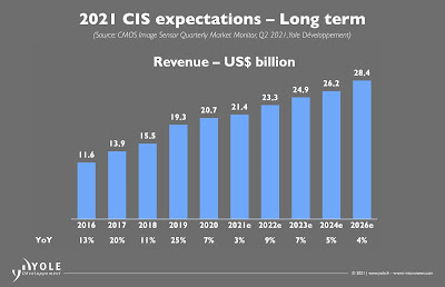
2020 saw CIS revenues reach $20.7B with an annual growth of 7.3%. As with other semiconductor products, Yole’s analysts noted that long production cycles and the activity of markets such as consumer, automotive, security, and industrial led to challenges in procurement of CIS at the end of 2020. In 2021, Yole’s imaging team expects a more stable situation. Q1-2021 has been very good due to some production overflow identified from Q4-2020, leading to a 7% better quarter compared to Q1-2020.

2020 was a very unusual year for the CIS industry. Everybody had the COVID-19 situation in mind, and, indeed, it created a temporary disruption in the supply chain which had to be made up towards year-end. Another disruptive aspect was the Huawei ban and its effect on the market between Q3 2020 and Q4 2020, especially for Sony. However, it did not lead to a CIS market collapse thanks to the increasing number of cameras per mobile and a stable average selling price overall.

All these events combined allowed for the CIS industry to maintain significant growth in 2020.


Q1 is seasonally a typically lower revenue quarter, though there was fear of shortages in the overall semiconductor industry,” explains Chenmeijing Liang, Technology & Market Analyst within the Photonics, Sensing & Display Division at Yole. “At Yole, we believe that the effect here is more linked to supply chain issues rather than real capacity issues for CIS.


Sony was hit the hardest by these crises, as it was highly exposed to the mobile market and subsequent international trade tensions; the toll on Sony’s revenue in Q4 2020 is notable,” asserts Pierre Cambou, Principal analyst in the Photonics and Sensing Division at Yole.

Sony, of course, remains the market leader, and though they did lose some market share in Q4-2020, they regained traction in Q1-2021. However, they are being challenged by increased competition. In comparison, their nearest competitor Samsung was more protected from this market shake-up due to its vertical integration. Their recently released line of 0.7µm pixel sensors targeting the mobile market helped them seize some of the new opportunities, with some OEMs, such as Xiaomi, benefiting from Huawei’s disappearance.

Some CIS fabless players, like ON Semiconductor, may not have the ability to secure capacity from TSMC, as Sony did. They did ok during 2020 but could have done better by surfing the automotive and logistic camera market growth.

But other fabless players, probably Chinese, like Smartsens Technology and Omnivision, diversified their sourcing long ago and grew far more.

PhotonicSens Promises 3D Image from Single Lens Camera Module

PRNewswire: Photonicsens presents its 3D single-lens camera design with Qualcomm:

"photonicSENS' single lens 3D depth sensing solution will be a game changer for smartphones," says Ann Whyte, President of photonicSENS, "The  3D depth camera reference designs of this collaboration are based on our single lens apiCAM technology that with a single device delivers simultaneously an RGB image and depth map to offer smartphone manufacturers the means to differentiate with enhanced photographic features, a 1.4Mpx depthmap, the lowest component count, lowest cost and the lowest power dissipation, as well as the best performance in any environment.   Snapdragon 888 is a clear leader, and we are excited to be working with Qualcomm Technologies to release our cutting-edge 3D sensing solution to market."

Thursday, June 24, 2021

Axcelis Ships 8MeV Ion Implanter to "Leading CIS Manufacturer in China"

PRNewswire:  Axcelis has shipped an 8MeV Purion VXE high energy ion implantation system to a "leading CMOS image sensor manufacturer located in China." This is the first Purion VXE shipped to this chipmaker.

EVP of Product Development, Bill Bintz, commented, "The Purion VXE was designed to address the specific needs of customers developing and manufacturing the most advanced CMOS image sensors. To optimize both performance and yield, these emerging image sensor devices require ultra-high energy implants with extremely precise and deep implant profiles, concurrent with ultra-low metal contamination levels. Building off of Axcelis' market leading LINAC technology, the Purion VXE uniquely addresses these customer needs."

IDTechEx on Emerging Sensor Technologies

IDTechEx CEO Raghu Das and analyst Matthew Dyson present their view on "Emerging Image Sensor Technologies 2021-2031."


Wednesday, June 23, 2021

Infineon and PMD Partner with ArcSoft for Under-Display ToF Turnkey Solution

BusinessWire: Infineon, PMD and ArcSoft are developing a turnkey solution that allows a ToF camera to work under the display of commercial smartphones. It will provide reliable IR images and 3D data for security-relevant applications like face authentication and mobile payment. The market for ToF solutions in smartphones is estimated to reach above 600M sensor units in 2025 with a CAGR of around 32% from 2021 onward, according to Strategy Analytics.

Time-of-Flight technology offers tremendous value for smartphones and in our daily lives by making electronic devices aware of the context in which we use them,” says Andreas Urschitz, Division President Power & Sensor Systems at Infineon. “In addition to our continuous technological achievements in terms of smaller size, reduced power consumption, and better 3D performance, our AI-enabled and secure under-display solution will provide a display design beautification for smartphone manufacturers.

To build powerful Time-of-Flight cameras, you need to have a deep understanding of the 3D data and how applications make use of it. That is why we are working closely with middleware partners and OEMs to provide them best in class ToF-algorithms, software, and high-quality 3D data to build their application on. The solution, that we are jointly developing with ArcSoft, allows our ToF cameras to see through displays while still meeting the requirements for secure face authentication in mobile phone unlock and mobile payment,” adds Bernd Buxbaum, CEO at PMD.

"The implementation of 3D ToF in mobile devices promises to spark the next wave of killer consumer applications, which is exactly why ArcSoft is excited to work with Infineon and pmdtechnologies," says Sean Bi, COO of ArcSoft. "By deeply integrating ToF cameras with ArcSoft's computer vision algorithms, under-display ToF can bring reliable facial recognition solutions and a superior full-screen experience to consumers. Relying on under-display ToF, ArcSoft will also enable more applications such as AR related, which mobile manufacturers value when deployed in support of new and exciting mobile apps.

Intevac Night Vision Sensor Development Attracts $23M Funding

BusinessWire: Intevac has received two additional Phase 1 development program awards in addition to the ManTech development award received from the Night Vision and Electronics Sensors Directorate during Q1 of 2021.

The ManTech award continues our work on the current CMOS camera developed in support of IVAS, targeting reduced power and cost, and improved performance. In the new awards announced today, the Enhanced Performance CIS award is aimed at further improving low-light performance for our next-generation CMOS camera, advancing from the current high-starlight operating capability to overcast starlight. The second of the two new awards, the Enhanced Performance EBAPS award, is aimed at significantly improved low-light performance utilizing Intevac’s ISIE19 EBAPS technology. This Enhanced Performance EBAPS award is designed to provide ISIE19 low-light performance down to overcast-starlight capability in a greatly reduced form factor required for this application.

If selected for Phase 2 development work on all three of these IVAS-supporting programs, funded development revenues for Intevac Photonics would total approximately $23M over a 36-month period.

Intevac’s digital night-vision sensors, based on its patented Electron Bombarded Active Pixel Sensor (EBAPS) technology, provide state-of-the-art capability to the most advanced avionic fighting platforms in the U.S. Department of Defense inventory.

Nissan Gives Away Free Licenses for its Thermal Imaging Patents for Use in Anti-COVID Applications

I missed this news first announced in December 2020 and then again in April 2021: Nissan is providing licenses free of charge for thermal imaging sensor technology developed by the company.

Nissan is licensing the low-cost technology under the terms of the IP Open Access Declaration Against COVID-19, which the company joined in May. By signing the declaration, Nissan agreed not to seek compensation nor assert any patent, utility model, design or copyright claim against any activities aimed at combatting the pandemic.

The licenses are for multiple products being developed by Chino Corp. and Seiko NPC Corp. Chino is using Nissan’s technology to develop, manufacture and sell non-contact body surface temperature measuring devices that can quickly detect high body surface temperatures.

Seiko NPC has developed sensors under a sublicense of the technology from IHI Aerospace Co., Ltd. These sensors are being used in non-contact body surface temperature measuring devices for multiple companies.

Nissan’s contactless temperature-measuring sensor detects infrared rays from an object or area. It can display images, such as temperature distributions, with a resolution of about 2000 pixels and can be manufactured at significantly lower cost than sensors made using conventional technologies.

Tuesday, June 22, 2021

Jabil Develops 360-deg ToF Camera Based on ADI Reference Design

BusinessWire: Jabil announces that its optical design center in Jena, Germany, is currently developing a novel omnidirectional sensor for robotic and industrial platforms. By combining a custom optical assembly with an innovative active illumination approach, a new 3D ToF depth sensor with an industry-leading 360° x 60° FOV is being developed (data sheet states 270deg x 60deg FOV). The ground-breaking, solid-state design is one of several sensing systems Jabil’s optical business unit (Jabil Optics) is designing to support lower-cost autonomous mobile robotics and collaborative robotics platforms.

A mission of Analog Devices is to enable the autonomous mobile robot revolution by providing high performance and highly differentiated signal chains that bridge the gap between the analog and digital worlds,” said Donnacha O’Riordan, director of ADI. “The Jabil omnidirectional sensor is one of the most innovative implementations of the ADI depth-sensing technology we have encountered. Jabil’s wide field-of-view, depth-sensing approach is opening up new possibilities for human interaction with robots.


Monday, June 21, 2021

International Image Sensor Workshop Registration Opens

2021 International Image Sensor Workshop (IISW 2021) registration is open now. The Workshop is an on-line virtual event this year, to be held on September 20-23. The details are explained in FAQ part on the bottom of the registration page:

GPixel Expands its Line Scan Sensors Family

Gpixel expands its GL product family with GL3504, a C-mount line scan image sensor targeting industrial inspection, logistics barcode scanning, and printing inspection.

GL3504 has two photosensitive pixel arrays: a 2048 x 4 resolution array with 7 μm x 7 μm square pixel size and a 4096 x 2 resolution array with 3.5 μm x 3.5 μm pixel size. Both monochromatic and color variants are offered. The color filter array on the 3.5 μm pixel line is Bayer type; The 7 μm pixel lines are RGB true color type.

GL3504 engineering samples can be ordered today for delivery in July, 2021.

ESPROS about Human Eye as a LiDAR

Espros publishes its CEO Beat De Coi's presentation at Autosens Detroit 2021 "The Human eye as an example for LiDAR."

"The performance of the human eye is awesome. It has a fantastic resolution, hence small objects can bee seen at long distances. It works very well in a huge brightness dynamic range and it is able to estimate distance. This in a system of two eyes and a dedicated computer system - the human vision system (HVS). There are many aspects of the HVS which outperforms any LiDAR system. However, the perfomance is based on a very clever designed system. Why not to use the human eye and the human vision system as an example for future LiDAR systems?"

Sunday, June 20, 2021

Megapixel ToF Imager with 35um Depth Resolution

IEEE Transactions on Pattern Analysis and Machine Intelligence publishes a paper "Exploiting Wavelength Diversity for High Resolution Time-of-Flight 3D Imaging" by Fengqiang Li, Florian Willomitzer, Muralidhar Madabhushi Balaji, Prasanna Rangarajan, and Oliver Cossairt from Northwestern University at Evanston, IL, and Southern Methodist University, Dallas, TX. The paper has also been publishes in Arxiv.org and IEEE Computer Society Digital Library.

"The poor lateral and depth resolution of state-of-the-art 3D sensors based on the time-of-flight (ToF) principle has limited widespread adoption to a few niche applications. In this work, we introduce a novel sensor concept that provides ToF-based 3D measurements of real world objects and surfaces with depth precision up to 35 μm and point cloud densities commensurate with the native sensor resolution of standard CMOS/CCD detectors (up to several megapixels). Such capabilities are realized by combining the best attributes of continuous wave ToF sensing, multi-wavelength interferometry, and heterodyne interferometry into a single approach. We describe multiple embodiments of the approach, each featuring a different sensing modality and associated tradeoffs."