Friday, May 31, 2024

VisEra moves towards IPO

From Yahoo Finance news: https://uk.news.yahoo.com/finance/news/tsmc-sells-shares-optical-sensor-015509757.html?guccounter=1

TSMC Sells Shares in Optical Sensor Unit Before Planned Spinoff

(Bloomberg) -- Taiwan Semiconductor Manufacturing Co. sold shares in VisEra Technologies Co. before a planned initial public offering of the image sensor provider.

Taiwan’s largest chipmaker sold 38 million shares in VisEra at NT$240 ($8.60) apiece, cutting its stake in the company to 73.9%, according to a filing to the Taiwan stock exchange Tuesday. It sold the stock to 17 investors, including Fidelity International, Singapore sovereign wealth fund GIC Pte and domestic institutions Cathay Life Insurance Co. and Fubon Life Insurance Co.

The transaction was to facilitate a proposed listing of VisEra in Taiwan, TSMC said in the filing without providing further details.

TSMC set up VisEra in 2003 together with Santa Clara, California-based OmniVision Technologies Inc. before buying out its partner in 2015. The company is now seeking to spin off the unit just as a boom in semiconductor demand drives a surge in prices of chipmakers and other companies that supply to the industry. TSMC’s shares have nearly doubled over the past 12 months, making it the world’s 10th most valuable company at about $589 billion.

Thursday, May 30, 2024

Is 3D stacking for CIS unnecessary?

A recent video from GalaxyCore discusses their single wafer CIS arguing against the need for 3D stacking for higher resolution:


GalaxyCore's innovative single-wafer, high-resolution CMOS image sensor solution solves the problem of incompatibility between logic circuits and pixel technology through FPPI process and unique circuit architecture. Without the need for stacking, this advancement reduces silicon usage while maintaining performance equivalent to stacked CIS. The world's first 32-megapixel single-wafer CIS is already in mass production, and the 50-megapixel CIS has also been unveiled.

Monday, May 27, 2024

XMC plans IPO

XMC CIS Technology Platform [https://www.xmcwh.com/en/site/nor_flash]

XMC builds a full-loop & one-stop CIS (CMOS Image Sensor) technology platform. XMC has mass production capability of high-performance, low-power image sensor products. This technology can be widely used in smartphones, automotive electronics, machine vision, professional imaging and other market segments.

TrendForce News: https://www.trendforce.com/news/2024/05/15/news-xmc-initiates-ipo-plan-potentially-becoming-chinas-first-hbm-foundry/

(Also on DigiTimes Asia, but paywalled: https://www.digitimes.com/news/a20240514PD200/xmc-ipo-china-foundry-market.html)

 XMC initiates IPO in Chinese competitive foundry market

NOR Flash manufacturer Wuhan Xinxin Semiconductor Manufacturing Co. (XMC) recently disclosed an IPO counseling filing with the Hubei Securities Regulatory Bureau, according to the official website of the China Securities Regulatory Commission. Its recently announced bidding project may indicate its ambition to become China’s first HBM foundry, according to the report by Chinese media Semi Insights.

As per information from its website, XMC provides 12-inch foundry services for NOR Flash, CIS, and Logic applications with processes of 40 nanometers and above. Originally a wholly-owned subsidiary of Yangtze Memory Technologies (YMTC), XMC announced in March its first external financing round, increasing its registered capital from approximately CNY 5.782 billion to about CNY 8.479 billion. Its IPO counseling filing also indicates that it is still majority-owned by YMTC, with a shareholding ratio of 68.1937%.

According to market sources cited in the same report, XMC’s initiation of external financing and IPO plan is primarily aimed at supporting the significant expansion during a crucial development phase for YMTC. Given the substantial scale of YMTC, completing an IPO within three years poses challenges. Therefore, XMC was chosen as the IPO entity to enhance financing channels.

It is noteworthy that XMC also announced its latest bidding project on HBM (High Bandwidth Memory) – related advanced packaging technology R&D and production line construction, according to local media.

The project indicates the company’s capability to apply three-dimensional integrated multi-wafer stacking technology to develop domestically produced HBM products with higher capacity, greater bandwidth, lower power consumption, and higher production efficiency. With plans to add 16 sets of equipment, XMC’s latest project aims to achieve a monthly output capacity of over 3000 wafers (12 inches), showing its ambition of becoming China’s first HBM foundry.

On December 3, 2018, XMC announced the successful development of its three-dimensional wafer stacking technology based on its three-dimensional integration technology platform. This marks a significant advancement for the company in the field of three-dimensional integration technology, enabling higher density and more complex chip integration.

Currently, XMC has made much progress in the research and development of three-dimensional integrated multi-wafer stacking technology, which has been evident in the successful development of three-wafer stacking technology, the application of three-dimensional integration technology in back-illuminated image sensors, advancements in HBM technology research and industrialization efforts, as well as breakthroughs in the 3D NAND project.

Saturday, May 25, 2024

Two New Jobs Submitted by Luxima

Luxima Technology

Arcadia, California, USA     Career page link

Junior position - Analog Design Engineer

Senior position - Staff Analog Design Engineer 

Friday, May 24, 2024

"Black Silicon" photodiodes

Title: Excellent Responsivity and Low Dark Current Obtained with Metal-Assisted Chemical Etched Si Photodiode

Author: Kexun Chen, Olli E. Setälä, Xiaolong Liu, Behrad Radfar, Toni P. Pasanen, Michael D. Serué, Juha Heinonen, Hele Savin, Ville Vähänissi

Affiliation: Aalto University, Finland

Abstract: Metal-assisted chemical etched (MACE, also known as MacEtch or MCCE) nanostructures are utilized widely in the solar cell industry due to their excellent optical properties combined with a simple and cost-efficient fabrication process. The photodetection community, on the other hand, has not shown much interest towards MACE due to its drawbacks including insufficient surface passivation, increased junction recombination, and possible metal contamination, which are especially detrimental to pn-photodiodes. Here, we aim to change this by demonstrating how to fabricate high-performance MACE pn-photodiodes with above 90% external quantum efficiency (EQE) without external bias voltage at 200–1000 nm and dark current less than 3 nA/cm2 at −5 V using industrially applicable methods. The key is to utilize an induced junction created by an atomic layer deposited highly charged Al2O3 thin film that simultaneously provides efficient field-effect passivation and full conformality over the MACE nanostructures. Achieving close to ideal performance demonstrates the vast potential of MACE nanostructures in the fabrication of high-performance low-cost pn-photodiodes.


Wednesday, May 22, 2024

Prophesee AMD collaboration on DVS FPGA devkit

Prophesee collaborates with AMD to deliver industry-first Event-based Vision solution running on leading, FPGA-based AMD Kria™ KV260 Vision AI Starter Kit

Developers can now take full advantage of Prophesee Event-based Metavision® sensor and AI
performance, power, and speed to create the next generation of Edge AI machine vision applications
running on AMD platforms.

PARIS - May 6, 2024 –Prophesee SA, inventor of the world’s most advanced neuromorphic vision systems, today announced that its Event-based Metavision HD sensor and AI are now available for use with the AMD Kria ™ KV260 Vision AI Starter Kit, creating a powerful and efficient combination to accelerate the development of advanced Edge machine vision applications. It marks the industry’s first Event-based Vision development kit compatible with an AMD platform, providing customers a platform to both evaluate and go to production with an industrial-grade solution for target applications such as smart city and machine vision, security cameras, retail analytics, and many others.

The development platform for the AMD Kria™ K26 System-on-Module (SOM), the KV260 Vision AI starter kit is built for advanced vision application development without requiring complex hardware design knowledge or FPGA programming skills. AMD Kria SOMs for edge AI applications provide a production-ready, energy-efficient FPGA-based device with enough I/O to speed up vision and robotics tasks at an affordable price point. Combined with the Prophesee breakthrough Event-based vision technology, machine vision system developers can leverage the lower latency and lower power capabilities of the Metavision platform to experiment and create more efficient, and in many cases not previously possible, applications compared to traditional frame-based vision sensing approaches.

A breakthrough plug-and-play Active Markers Tracking application is included in this kit. It allows for >1,000Hz 3D pose estimation, with complete background rejection at pixel level while providing extreme robustness to challenging lighting conditions.

This application highlights unique features of Prophesee’s Event-based Metavision technologies, enabling a new range of ultra high-speed tracking use cases such as game controller tracking, construction site safety, heavy load anti-sway systems and many more.

Multiple additional ready-to-use application algorithms will be made available over the coming months.

The Prophesee Starter Kit provides an ‘out of the box’ development solution to quickly get up and running with the Prophesee Metavision SDK and IMX636 HD Event-based sensor realized in collaboration between Prophesee and Sony, allowing easy porting of algorithms to the AMD commercial and industrial-grade system-on-module (SOMs) powered by the custom-built Zynq™ UltraScale+™ multiprocessing SoC.

The new, Prophesee-enabled Kria KV260 AI Starter Kit will be on display at Automate 2024 in
Prophesee’s booth 3452

“The ever-expanding Kria ecosystem helps make motion capture, connectivity, and edge AI applications more accessible to roboticists and developers,” said Chetan Khona, senior director of Industrial, Vision, Healthcare and Sciences Markets, AMD. “Prophesee Event-based Vision offers unique advantages for machine vision applications. Its low data consumption translates into efficient energy consumption, less compute and memory needed, and fast response times.”

“It’s never been easier to develop Event-based Edge applications with this combination of development aids from AMD and Prophesee,” said Luca Verre, co-founder and CEO of Prophesee. “We are providing everything needed to take complete advantage of the lower power processing and low latency performance inherent in Event-based Vision, as well as provide an environment to optimize machine vision system based on specific KPIs for customer-defined applications and use cases. This will further accelerate the adoption of Event-based Vision in key market segments that can benefit from Metavision’s unique advantages.”

https://www.prophesee.ai/event-based-metavision-amd-kria-starter-kit-imx636/


Monday, May 20, 2024

PixArt far infrared sensors - 3 part video series


 This video is the first episode of the Far Infrared (FIR) sensor series, focusing on the basic concepts of FIR and highlighting the differences between traditional thermistor and FIR thermopile.


This video is the second episode of the Far Infrared (FIR) sensor series, introducing PixArt's range of FIR sensor product lines. In addition to single point and 64-pixel array sensors, PixArt also provides a powerful 3-in-1 evaluation board that integrates a range of automated thermal detection functions.


This video is the third episode of the Far Infrared (FIR) sensor series, featuring demonstrations of 3 FIR sensors. In addition to showcasing real-life scenarios using PixArt’s FIR sensors, it also introduces various applications in different fields.

Sunday, May 19, 2024

Job Postings - Week of 19 May 2024

Onsemi

Product Engineer

Nampa, Idaho, USA

Link

Qualcomm

Camera Sensor System Engineer, Senior to Staff

Taipei City, Taiwan

Link

Apple

Hardware Sensing Systems Engineer

San Diego, California, USA

Link

Qualcomm

Sr Engineer-Camera Sensor

Hyderabad, Telangana, India

Link

L3Harris Technologies - WESCAM

Principal, Product Management

Waterdown, Ontario, Canada

Link

NASA Postdoc

Infrared Detector Technology Development

Pasadena, California, USA

Link

FRAMOS

Account Manager, Americas

Ottawa, Ontario, Canada

Link

Diamond Light Source

PDRA High-Z sensors and charge integrating detectors – Postdoc

Didcot, Oxfordshire, England

Link

Omnivision

Sr. Field Applications Engineer

Fleet, Hampshire, England

Link

A DIY copper oxide camera sensor

Can we make photosensitive pixels from Copper Oxide? Youtuber "Breaking Taps" answers:


Friday, May 17, 2024

One man's (event camera) noise is another man's signal

In a preprint titled "Noise2Image: Noise-Enabled Static Scene Recovery for Event Cameras" Cao et al. propose a method to use the inherent pixel noise present in even camera sensors to recover scene intensity maps.

Abstract:

Event cameras capture changes of intensity over time as a stream of ‘events’ and generally cannot measure intensity itself; hence, they are only used for imaging dynamic scenes. However, fluctuations
due to random photon arrival inevitably trigger noise events, even for static scenes. While previous efforts have been focused on filtering out these undesirable noise events to improve signal quality, we find that,
in the photon-noise regime, these noise events are correlated with the static scene intensity. We analyze the noise event generation and model its relationship to illuminance. Based on this understanding, we propose a method, called Noise2Image, to leverage the illuminance-dependent noise characteristics to recover the static parts of a scene, which are otherwise invisible to event cameras. We experimentally collect a dataset of noise events on static scenes to train and validate Noise2Image. Our results show that Noise2Image can robustly recover intensity images solely from noise events, providing a novel approach for capturing static scenes in event cameras, without additional hardware.

Link: https://arxiv.org/abs/2404.01298


Wednesday, May 15, 2024

Photonic-electronic integrated circuit-based coherent LiDAR engine

Lukashchuk et al. recently published a paper titled "Photonic-electronic integrated circuit-based coherent LiDAR engine" in the journal Nature Communications.

Open access link: https://www.nature.com/articles/s41467-024-47478-z

Abstract: Chip-scale integration is a key enabler for the deployment of photonic technologies. Coherent laser ranging or FMCW LiDAR, a perception technology that benefits from instantaneous velocity and distance detection, eye-safe operation, long-range, and immunity to interference. However, wafer-scale integration of these systems has been challenged by stringent requirements on laser coherence, frequency agility, and the necessity for optical amplifiers. Here, we demonstrate a photonic-electronic LiDAR source composed of a micro-electronic-based high-voltage arbitrary waveform generator, a hybrid photonic circuit-based tunable Vernier laser with piezoelectric actuators, and an erbium-doped waveguide amplifier. Importantly, all systems are realized in a wafer-scale manufacturing-compatible process comprising III-V semiconductors, silicon nitride photonic integrated circuits, and 130-nm SiGe bipolar complementary metal-oxide-semiconductor (CMOS) technology. We conducted ranging experiments at a 10-meter distance with a precision level of 10 cm and a 50 kHz acquisition rate. The laser source is turnkey and linearization-free, and it can be seamlessly integrated with existing focal plane and optical phased array LiDAR approaches.


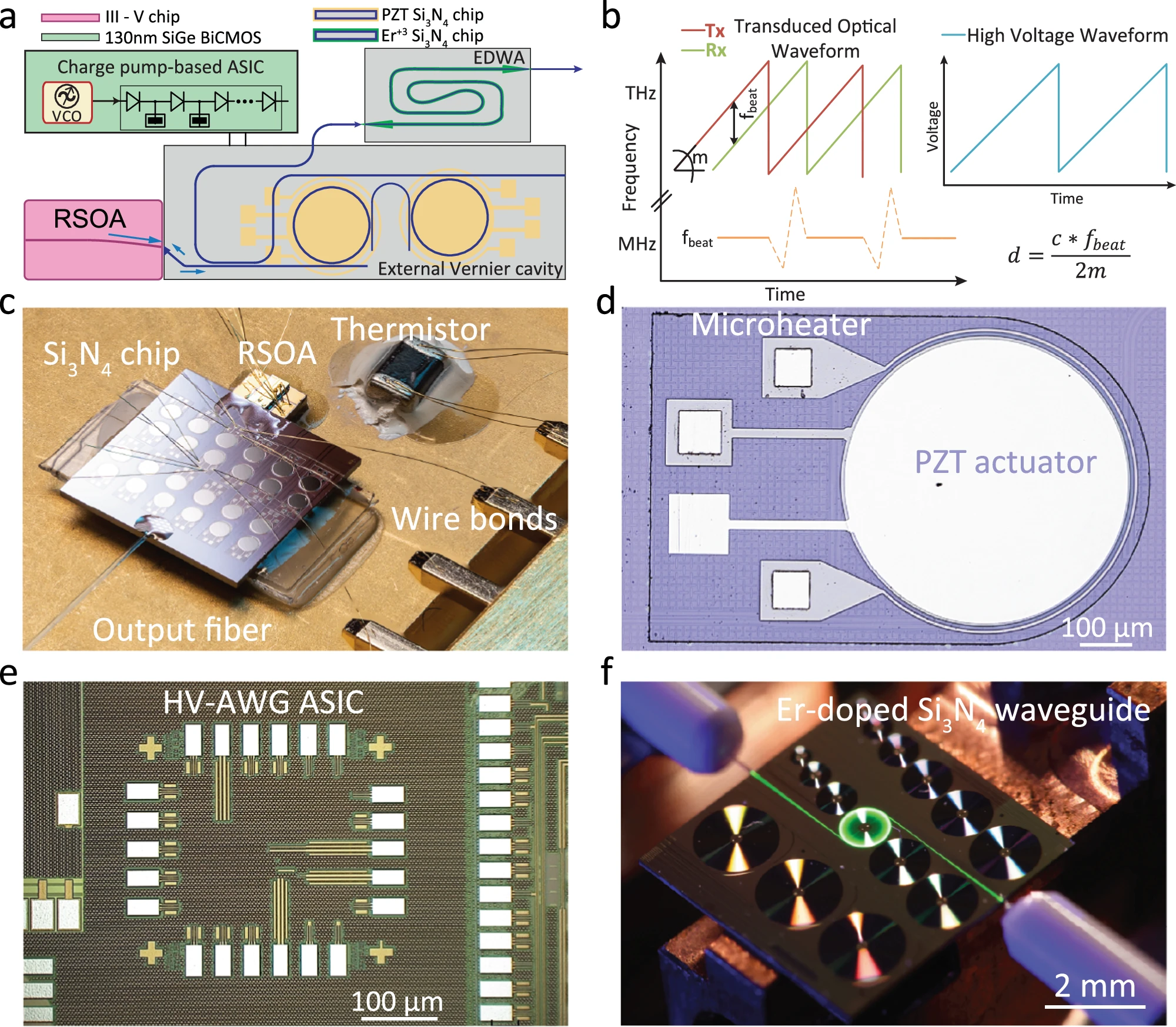
a Schematics of photonic-electronic LiDAR structure comprising a hybrid integrated laser source, charge-pump based HV-AWG ASIC, photonic integrated erbium-doped waveguide amplifier. b Coherent ranging principle. c Packaged laser source. RSOA is edge coupled to Si3N4 Vernier filter configuration waveguide, whereas the output is glued to the fiber port. PZT and microheater actuators are wirebonded as well as butterfly package thermistor. d Zoom-in view of (c) highlighting a microring with actuators. e Micrograph of the HV-AWG ASIC chip fabricated in a 130 nm SiGe BiCMOS technology. The total size of the chip is 1.17–1.07 mm2. f The Erbium-doped waveguide is optically excited by a 1480 nm pump showing green luminescence due to the transition from a higher lying energy level to the ground state.

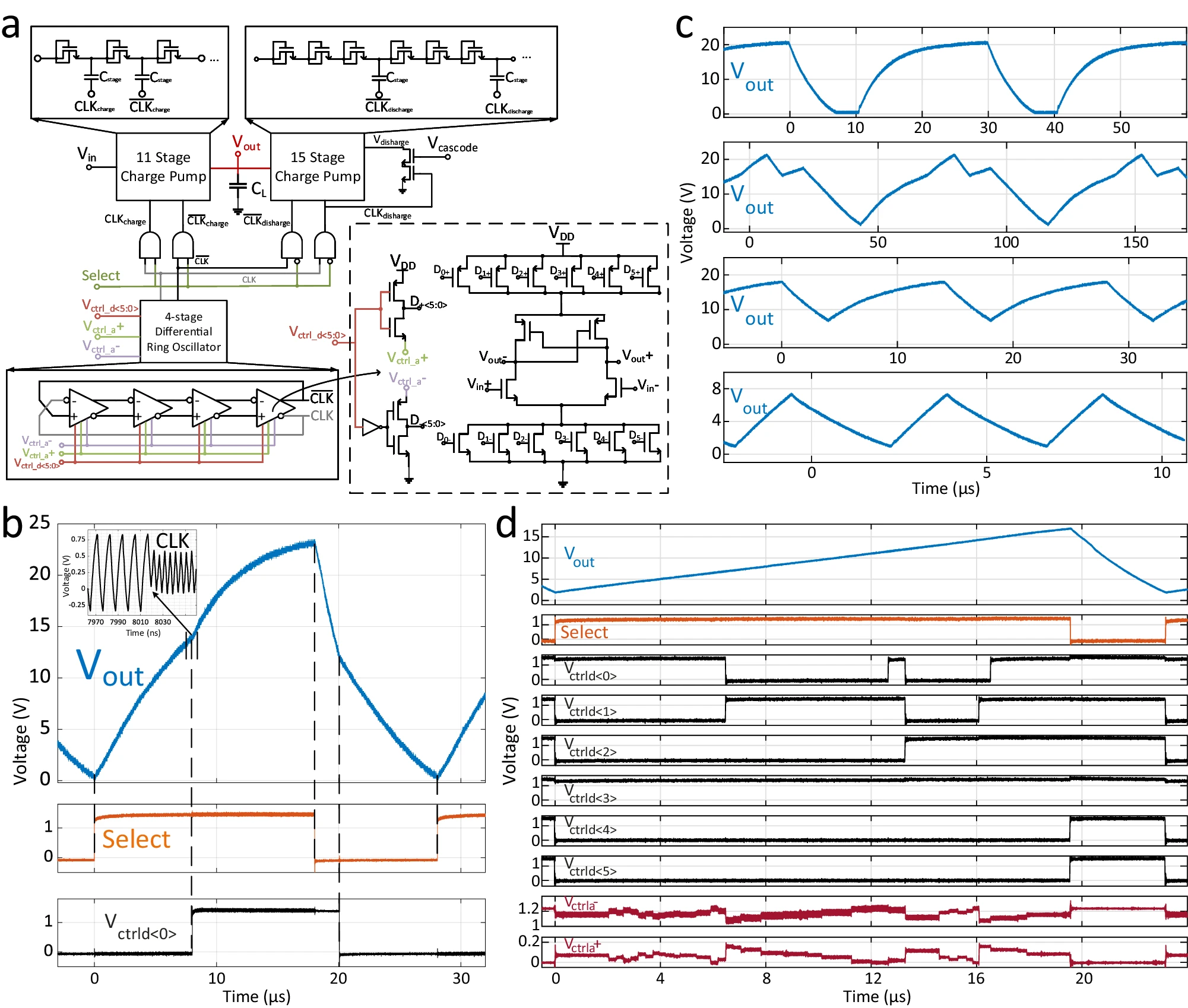
a Schematics of the integrated circuit consisting of a 4-stage voltage-controlled differential ring oscillator which drives charge pump stages to generate high-voltage arbitrary waveforms. b Principles of waveform generation demonstrated by the output response to the applied control signals in the time domain. Inset shows the change in oscillation frequency in response to a frequency control input, from 88 MHz to 208 MHz, which modifies the output waveform. c Measured arbitrary waveforms generated by the ASIC with different shapes, amplitudes, periods and offset values. d Generation of the linearized sawtooth electrical waveform used in LiDAR measurements. Digital and analog control signals are modulated in the time domain to fine-tune the output. 

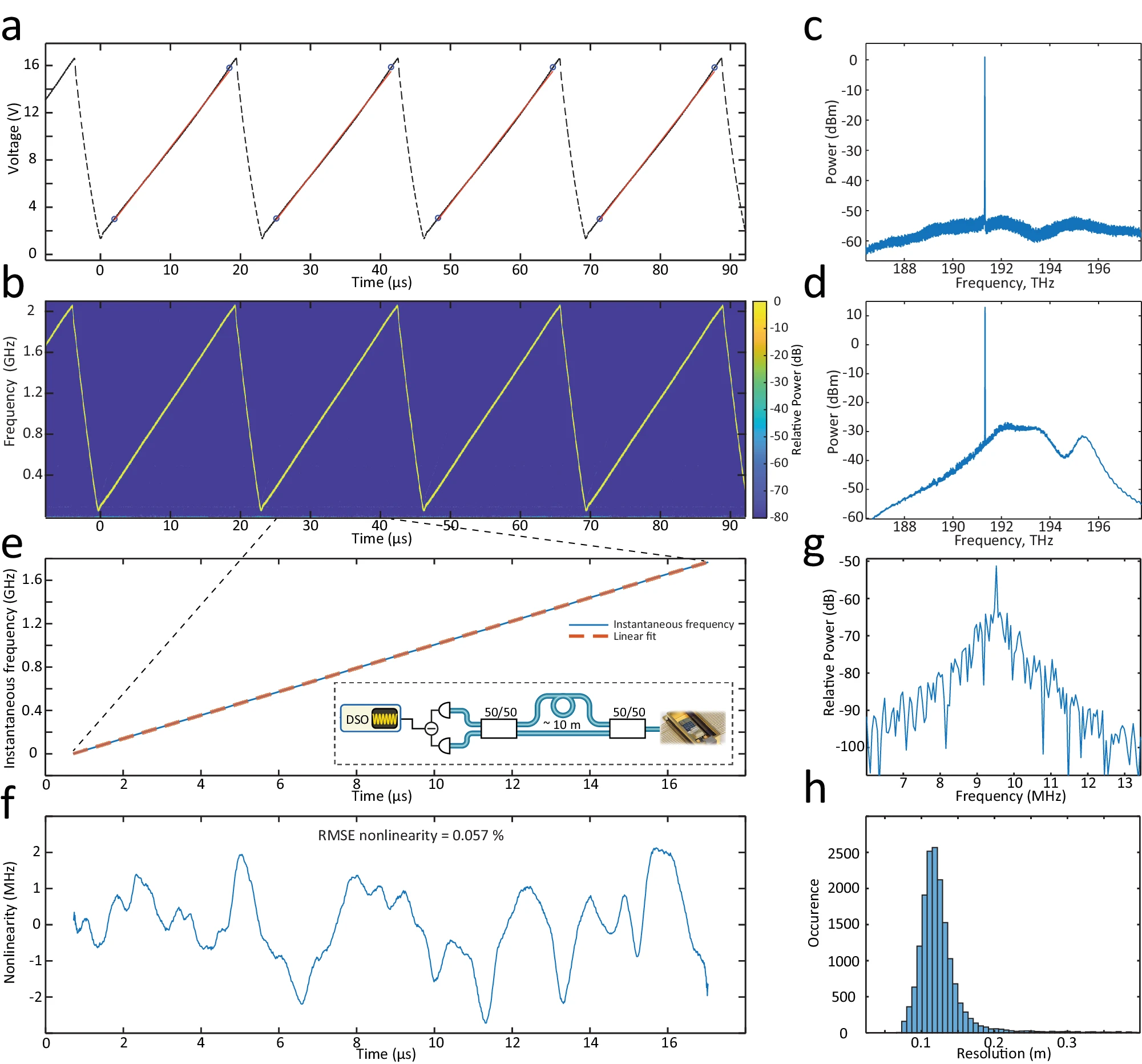
a Electrical waveform generated by the ASIC. Blue circles highlight the segment of ~ 16 μs used for ranging and linearity analysis. The red curve is a linear fit to the given segment. b Time-frequency map of the laser chirp obtained via heterodyne detection with auxiliary laser. RBW is set to 10 MHz. c Optical spectrum of Vernier laser output featuring 50 dB side mode suppression ratio. d Optical spectrum after EDWA with >20 mW optical power. e Instantaneous frequency of the optical chirp obtained via delayed homodyne measurement (inset: experimental setup). The red dashed line corresponds to the linear fit. The excursion of the chirp equates to 1.78 GHz over a 16 μs period. f Nonlinearity of the laser chirp inferred from (e). RMSE nonlinearity equates to 0.057% with the major chirp deviation from the linear fit lying in the window ± 2 MHz. g The frequency beatnote in the delayed homodyne measurement corresponds to the reference MZI delay ~10 m. The 90% fraction of the beatnote signal is taken for the Fourier transformation. h LiDAR resolution inferred from the FWHM of the MZI beatnotes over >20,000 realizations. The most probable resolution value is 11.5 cm, while the native resolution is 9.3 cm corresponding to 1.61 GHz (90% of 1.78 GHz).

a 
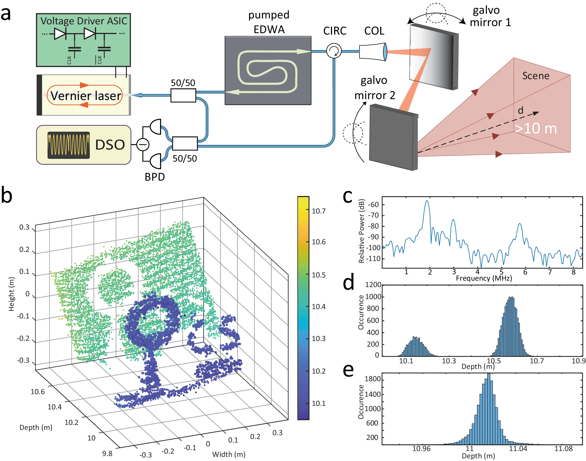
Schematics of the experimental setup for ranging experiments. The amplified laser chirp scans the target scene via a set of galvo mirrors. A digital sampling oscilloscope (DSO) records the balanced detected beating of the reflected and reference optical signals. CIRC - circulator, COL - collimator, BPD - balanced photodetector. b Point cloud consisting of ~ 104 pixels featuring the doughnut on a cone and C, S letters as a target 10 m away from the collimator. c The Fourier transform over one period, highlighting collimator, circulator and target reflection beatnotes. Blackman-Harris window function was applied to the time trace prior to the Fourier transformation. d Detection histogram of (b). e Single point imaging depth histogram indicating 1.5 cm precision of the LiDAR source.
 

Monday, May 13, 2024

SI Sensors introduces custom CIS design services

Custom CMOS image sensor design on a budget
 
Specialised Imaging Ltd reports on the recent market launch of SI Sensors (Cambridge, UK) - a new division of the company focused on the development of advanced CMOS image sensors.
 
Drawing upon a team of specialists with a broad range of experience in image sensor design – SI Sensors is creating custom image sensor designs with cutting edge performance. In particular, the company’s in-house experts have specialist knowledge of visible and non-visible imaging technologies, optimised light detection and charge transfer, radiation-hard sensor design, and creating CCD-in-CMOS pixels to enable novel imaging techniques such as ultra-fast burst mode imaging.
 
Philip Brown, General Manager of SI Sensors said, “In addition to developing new sensors for Specialised Imaging’s next generation of ultra-fast imaging cameras utilising the latest foundry technologies, we are developing solutions for other customers with unique image sensor design requirements including for space and defence applications”.
 
He added “SI Sensors team also use their skills and experience to develop bespoke image sensor packages that accommodate custom electrical, mechanical, and thermal interface requirements. Our aim is always to achieve the best balance between image sensor performance and cost (optimised value) for customers. To ensure performance and consistent quality and reliability we perform detailed electro-optical testing from characterisation through to mass production testing adhering to industry standards such as EMVA 1288”.
 
For further information on custom CMOS image sensor design and production please visit www.si-sensors.com or contact SI Sensors on +44-1442-827728 or info@si-sensors.com.
 
Specialised Imaging Ltd is a dynamic company focused on niche imaging markets and applications, with particular emphasis on high-speed image capture and analysis. Drawing upon over 20 years’ experience, Specialised Imaging Ltd today are market leaders in the design and manufacture of ultra-fast framing cameras and ultra high-speed video cameras.

Friday, May 10, 2024

NASA develops a 36 pixel sensor

From PetaPixel: https://petapixel.com/2024/04/30/nasa-develops-tiny-yet-mighty-36-pixel-sensor/

NASA Develops Tiny Yet Mighty 36-Pixel Sensor


While NASA’s James Webb Space Telescope is helping astronomers craft 122-megapixel photos 1.5 million kilometers from Earth, the agency’s newest camera performs groundbreaking space science with just 36 pixels. Yes, 36 pixels, not 36 megapixels.

The X-ray Imaging and Spectroscopy Mission (XRISM), pronounced “crism,” is a collaboration between NASA and the Japan Aerospace Exploration Agency (JAXA). The mission’s satellite launched into orbit last September and has been scouring the cosmos for answers to some of science’s most complex questions ever since. The mission’s imaging instrument, Resolve, has a 36-pixel image sensor.

This six-by-six pixel array measures 0.2 inches (five millimeters) per side, which is not so different from the image sensor in the Apple iPhone 15 and 15 Plus. The main camera in those smartphones is eight by six millimeters, albeit with 48 megapixels. That’s 48,000,000 pixels, just a handful more than 36.

How about a full-frame camera, like the Sony a7R V, the go-to high-resolution mirrorless camera? That camera has over 60 megapixels and captures images that are 9,504 by 6,336 pixels. The image sensor has a total of 60,217,344 pixels, 1,672,704 times the number of pixels in XRISM’s Resolve imager.

At this point, it is reasonable to wonder, “What could scientists possibly see with just 36 pixels?” As it turns out, quite a lot.

Resolve detects “soft” X-rays, which are about 5,000 times more energetic than visible light wavelengths. It examines the Universe’s hottest regions, largest structures, and most massive cosmic objects, like supermassive black holes. While it may not have many pixels, its pixels are extraordinary and can produce a rich spectrum of visual data from 400 to 12,000 electron volts.

“Resolve is more than a camera. Its detector takes the temperature of each X-ray that strikes it,” explains Brian Williams, NASA’s XRISM project scientist at Goddard. “We call Resolve a microcalorimeter spectrometer because each of its 36 pixels is measuring tiny amounts of heat delivered by each incoming X-ray, allowing us to see the chemical fingerprints of elements making up the sources in unprecedented detail.”

Put another way, each of the sensor’s 36 pixels can independently and accurately measure changes in temperature of specific wavelengths of light. The sensor measures how the temperature of each pixel changes based on the X-ray it absorbs, allowing it to measure the energy of a single particle of electromagnetic radiation.

There is a lot of information in this data, and scientists can learn an incredible amount about very distant objects based using these X-rays.

Resolve can detect particular wavelengths of light so precisely that it can detect the motions of individual elements within a target, “effectively providing a 3D view.” The camera can detect the flow of gas within distant galaxy clusters and track how different elements behave within the debris of supernova explosions.

The 36-pixel image sensor must be extremely cold during scientific operations to pull off this incredible feat.

Videographers may attach a fan to their mirrorless camera to keep it cool during high-resolution video recording. However, for an instrument like Resolve, a fan just won’t cut it.
Using a six-stage cooling system, the sensor is chilled to -459.58 degrees Fahrenheit (-273.1 degrees Celsius), which is just 0.09 degrees Fahrenheit (0.05 degrees Celsius) above absolute zero. By the way, the average temperature of the Universe itself is about -454.8 degrees Fahrenheit (-270.4 degrees Celsius).

While a 36-pixel camera helping scientists learn new things about the cosmos may sound unbelievable, “It’s actually true,” says Richard Kelley, the U.S. principal investigator for XRISM at NASA’s Goddard Space Flight Center in Greenbelt, Maryland.

“The Resolve instrument gives us a deeper look at the makeup and motion of X-ray-emitting objects using technology invented and refined at Goddard over the past several decades,” Kelley continues.

XRISM and Resolve offer the most detailed and precise X-ray spectrum data in the history of astrophysics. With just three dozen pixels, they are charting a new course of human understanding through the cosmos (and putting an end to the megapixel race).

Talk on Digital Camera Myths and Misunderstandings - Part II

In a follow-up to the talk that was previously shared on this blog, here's Digital Camera Myths, Misstatements and Misunderstandings Part II, a presentation by Wayne Prentice to Rochester, NY chapter of IS&T (Society for imaging Science and Tech.) on 17 April. 2024. 


00:00 - Introduction
5:51 - Revisiting ISO sensitivity
9:12 - 12 ISO 10/Ha - really independent of camera and illuminant?
13:49 - "It's official: ISO 51,200 is the new 6400". Really?
22:44 - RCCB (Red, clear, clear Blue) sensors yield better SNR. Really?
25:35 - Depth of field: should you always use a longer focal length?
28:18 - sRGB, gamma, CRT display, and Human Vision
31:00 - Questions

Tuesday, May 07, 2024

NIT announces new full HD SWIR sensor - NSC2101

New High-Resolution, SWIR Sensor with High Performance

NIT (New Imaging Technologies) introduces its latest innovation in SWIR imaging technology: a high-resolution Short-Wave Infrared (SWIR) InGaAs sensor designed for the most demanding challenges in the field.

Overview
The new SWIR sensor – NSC2101 boasts remarkable features, including a high-performance InGaAs sensor with an 8µm pixel pitch, delivering an impressive 2MPIX resolution at 1920x1080px. Its ultra-low noise of only 25e- ensures exceptional image clarity, even in challenging environments. Additionally, with a dynamic range of 64dB, the sensor captures a wide spectrum of light intensities with precision and accuracy.

•    0.9µm to 1.7µm spectrum
•    2MPix – 1920x1080px @8µm pixel pitch
•    25e- readout noise
•    64dB dynamic range
This cutting-edge sensor is designed and manufactured by NIT in France and promises unparalleled performance and reliability. Leveraging advanced technology and expertise, NIT has crafted a sensor that meets the rigorous standards of ISR applications, offering crucial insights and intelligence in various scenarios.

Image examples


Applications
The applications of this SWIR sensor are vast and diverse, catering to the needs of defense, security, and surveillance industries. The sensor’s capabilities are indispensable for enhancing situational awareness and decision-making, from monitoring border security to providing critical intelligence in tactical operations.

Extension
Moreover, NIT’s commitment to innovation extends beyond the sensor itself. The camera version, integrating the NSC2101 sensor, will be released soon, this summer

Monday, May 06, 2024

Job Postings - Week of 5 May 2024

UC Santa Cruz

Systems Design and Characterization Engineer

Santa Cruz, California, USA

Link

FAPESP - São Paulo Research Foundation

Young Investigator Position in Quantum Technologies

São Paulo, Brazil

Link

Apple

Pixel Development Engineer

Cupertino, California, USA

Link

Meta – Facebook App

Sensor Application Engineer

Sunnyvale, California, USA

Redmond, Washington, USA

Link

University of Houston

Postdoctoral/Senior Research Scientist-X-ray, photon counting detectors

Houston, Texas, USA

Link

IRFU

Staff position in detector physics at CEA/IRFU/DEDIP

Saclay, France

Link

NASA

Development of infrared detectors and focal plane arrays for space instruments

Pasadena, California, USA

Link

Forvia-Faurecia

ADAS Camera Systems Engineer

Northville, Michigan, USA

Link

University of Edinburgh

Sensor and Imaging Systems MSc 

Edinburgh, Scotland, UK

Link

Friday, May 03, 2024

Foveon sensor development "still in design stage"

https://www.dpreview.com/interviews/6004010220/sigma-full-frame-foveon

Full-frame Foveon sensor "still at design stage" says Sigma CEO, "but I'm still passionate"

"Unfortunately, we have not made any significant progress since last year," says Sigma owner and CEO Kazuto Yamaki, when asked about the planned full-frame Foveon camera. But he still believes in the project and discussed what such a camera could still offer.

"We made a prototype sensor but found some design errors," he says: "It worked but there are some issues, so we re-wrote the schematics and submitted them to the manufacturer and are waiting for the next generation of prototypes." This isn't quite a return to 'square one,' but it means there's still a long road ahead.

"We are still in the design phase for the image sensor," he acknowledges: "When it comes to the sensor, the manufacturing process is very important: we need to develop a new manufacturing process for the new sensor. But as far as that’s concerned, we’re still doing the research. So it may require additional time to complete the development of the new sensor."

The Foveon design, which Sigma now owns, collects charge at three different depths in the silicon of each pixel, with longer wavelengths of light able to penetrate further into the chip. This means full-color data can be derived at each pixel location rather than having to reconstruct the color information based on neighboring pixels, as happens with conventional 'Bayer' sensors. Yamaki says the company's thinking about the benefits of Foveon have changed.

"When we launched the SD9 and SD10 cameras featuring the first-generation Foveon sensor, we believed the biggest advantage was its resolution, because you can capture contrast data at every location. Thus we believed resolution was the key." he says: "Today there are so many very high pixel-count image sensors: 60MP so, resolution-wise there’s not so much difference."

But, despite the advances made elsewhere, Yamaki says there's still a benefit to the Foveon design "I’ve used a lot of Foveon sensor cameras, I’ve taken a bunch of pictures, and when I look back at those pictures, I find a noticeable difference," he says. And, he says, this appeal may stem from what might otherwise be seen as a disadvantage of the design.

"It could be color because the Foveon sensor has lots of cross-talk between R, B and G," he suggests: "In contrast, Bayer sensors only capture R, B and G, so if you look at the spectral response a Bayer sensor has a very sharp response for each color, but when it comes to Foveon there’s lots of crosstalk and we amplify the images. There’s lots of cross-talk, meaning there’s lots of gradation between the colors R, B and G. When combined with very high resolution and lots of gradation in color, it creates a remarkably realistic, special look of quality that is challenging to describe."

The complexity of separating the color information that the sensor has captured is part of what makes noise such a challenge for the Foveon design, and this is likely to limit the market, Yamaki concedes:
"We are trying to make our cameras with the Foveon X3 sensor more user-friendly, but still, compared to the Bayer sensor cameras, it won’t be easy to use. We’re trying to improve the performance, but low-light performance can’t be as good as Bayer sensor. We will do our best to make a more easy-to-use camera, but still, a camera with Foveon sensor technology may not be the camera for everybody."

But this doesn't dissuade him. "Even if we successfully develop a new X3 sensor, we may not be able to sell tons of cameras. But I believe it will still mean a lot," he says: "despite significant technology advancements there hasn't been much progress in image quality in recent years. There’s a lot of progress in terms of burst rate or video functionality, but whe
n you talk just about image quality, about resolution, tonality or dynamic range, there hasn’t been so much progress."

"If we release the Foveon X3 sensor today and people see the quality, it means a lot for the industry, that’s the reason I’m still passionate about the project."