Sunday, February 28, 2021

Image Sensors on NASA Perseverance Rover

IMVEurope publishes "The sensor stories behind the Mars Perseverance images" based on talks with Guy Meynants, CMOSIS co-founder, and Paul Jerram of Teledyne e2v.

"Belgian firm Cmosis built its CMV20000 sensor originally as a custom product for traffic monitoring, releasing it in the summer of 2012, around the time when Perseverance's predecessor, Curiosity, was touching down on Mars.

Early in 2013 an internal study looked at ways of modernising the engineering cameras that had flown on Curiosity, as the design of those cameras was at that time more than 20 years old.

One of the upgrades was to use the CMV20000 20-megapixel sensor in the engineering cameras, the navigation and hazard detection eyes of the rover. Guy Meynants, one of the founders of Cmosis and now working for image sensor firm Photolitics, told Imaging and Machine Vision Europe that JPL initially requested information about the sensors much like any other customer, but at that time the team at Cmosis didn't know what it would be used for.

Then, later on, 'we started to get very specific questions, which came to me,' Meynants recalled. 'There was some urgency, and I was CTO at Cmosis at the time. It was then that we started to realise it might be used for something like this [the Mars rover].'

The cameras on Perseverance have three main improvements over those that flew on Curiosity, say the JPL scientists in the Space Science Reviews paper. Firstly, the Cmosis CMV20000 sensors are colour chips, which gives better contextual imaging capabilities than the monochrome predecessors. The second improvement is that the cameras have a wider field of view – 90° x 70° as opposed to 45° x 45° – which means only five overlapping images are needed to create a 360° panoramic view (Curiosity needed 10 images to achieve the same effect). The third improvement is that the 20-megapixel sensors can resolve greater detail than the older model.

In terms of the analytical instruments onboard the rover, a combination of CMOS and CCD detectors are used. Cmosis has a sensor – CV4000, a 2k x 2k device – in the Supercam, which will examine the chemical composition of rocks and soil. Meynants said that the route to include CV4000 in Supercam was a more classical space science project, with a full qualification of the microlenses and scientific work on whether the sensor was suited to the task.

Supercam also contains a CCD from Teledyne e2v, part of Teledyne Imaging, as does the Sherloc instrument – Scanning Habitable Environments with Raman and Luminescence for Organics and Chemicals – which will look for minerals, organic molecules and potential biosignatures. Teledyne Imaging companies also produced key optical components for the Sherloc UV spectrometer, including many of the lenses and mirrors.

Both the Teledyne CCDs on Supercam and Sherloc are 2k wide by 512 pixels high. Here, sensitivity is key, in the visible spectrum but also out into the UV and infrared, according to Paul Jerram, chief engineer at Teledyne e2v.

Jerram told Imaging and Machine Vision Europe that this particular CCD has a heritage stretching back to the early 1990s. It was originally made for the Royal Greenwich Observatory as a large area detector. After that, what was then e2v made variants of the detector for spectroscopy.

A version of the sensor was used onboard Curiosity, so the work for Perseverance had to some extent already been proven. 'We provide a detector that's really efficient,' Jerram said, almost 100 per cent detection efficiency. The signal returning to the detector from pulses of laser light is not huge, and instruments like Supercam and Sherloc need a sensor with very low noise that captures all of the signal."

Saturday, February 27, 2021

WaveTouch Sues Goodix and Huawei over Under-Screen Optical Fingerprint Patent Infringement

GizomoChina reports that UK-headquartered WaveTouch has filed claims against Goodix and Huawei over infringement on its optical fingerprint patents. WaveTouch Group Ltd. is a Joint Venture between OPDI Technologies A/S, Denmark and O-Net Communications Limited, Hong Kong. The Wavetouch technology is developed by OPDI Technologies A/S in partnership with the Technical University of Denmark (DTU), Denmark and Presto Engineering, Denmark.

Jørgen Korsgaard Jensen, founder of WaveTouch says that he has “always been very much in favor of establishing [a] close and good cross border relationship between Europe and China as I think the mix of different backgrounds and cultures can create innovative solutions and ideas. Today, the majority of employees in WaveTouch are employed in our Shenzhen based subsidiary and in this light it saddens me even more to see this kind of behavior disrespecting intellectual property rights.

WaveTounch news release says "We are incredibly pleased to announce, that Wavetouch’s main patent application, regarding our ultra-thin in-display fingerprint sensor technology, has now been granted in Europe. This technology has been designed for all high-end smartphones, due to the high-resolution and high contrast image of the actual fingerprint.

We expect similar grants, in the rest of the world, within a foreseeable future."

GizChina: The lawsuit is filed in a court in Dusseldorf, Germany. It's not clear which patent is in the dispute but WaveTouch has a number of patent applications on fingerprint sensor under OLED display, such as US20200285345:

Friday, February 26, 2021

ISSCC 2021: Samsung iToF Sensor

Samsung presents "A 4-tap 3.5μm 1.2Mpixel Indirect Time-of-Flight CMOS Image Sensor with Peak Current Mitigation and Multi-User Interference Cancellation" by Min-Sun Keel, Daeyun Kim, Yeomyung Kim, Myunghan Bae, Myoungoh Ki, Bumsik Chung, Sooho Son, Hoyong Lee, Heeyoung Jo, Seung-Chul Shin, Sunjoo Hong, Jaeil An, Yonghun Kwon, Sungyoung Seo, Sunghyuck Cho, Youngchan Kim, Young-Gu Jin, Youngsun Oh, Yitae Kim, JungChak Ahn, Kyoungmin Koh, Yongin Park.

Image Sensor Packaging Video

AIM Micro Systems publishes a promotional video showing different technologies and equipment involved in image sensor packaging:

Thursday, February 25, 2021

Velodyne Founder Responds to Board Decision

BusinessWire: David Hall, who with Marta Thoma Hall holds voting control of approximately 58.4% of the outstanding common stock of Velodyne Lidar, Inc. issued the following statement in response to the Company’s February 22, 2021 announcement:

As Board members and large stockholders, Marta and I have acted ethically and tirelessly to advance the best interests of Velodyne Lidar. We presided over years of growth and success that ultimately laid the groundwork for Velodyne Lidar to go public via a reverse merger in 2020. Since Anand Gopalan assumed the Chief Executive Officer role early last year, I have stepped back from day-to-day management and offered strategic perspectives when appropriate. I ultimately relinquished my Executive Chairman position in favor of simply serving as Chairman once it became clear this winter that Mr. Gopalan and others preferred to continuously ignore my input in favor of implementing their own agenda.

Marta and I firmly believe that the boardroom ambush that took place on February 19, 2021 is an affront to stockholders that undermines corporate democracy. The Board’s rash decision to censure us based on an opaque, secret investigation into baseless, unfounded claims simply reveals that the Company’s governance is broken. Moreover, stripping us of our respective positions – without justification – after many years of success appears more like an internal power grab than a pro-stockholder action. We are committed to righting these wrongs in the weeks ahead and plan to communicate substantive updates in the near-term.

SiOnyx vs Hamamatsu Oral Argument

US Federal Circuit Court publishes the oral arguments between Hamamatsu and SiOnyx lawyers, a nice example of how these lawsuits are managed. One can listen and decide which side sounds more convincing:

TechInsights Webinar on CIS Trends Learned from Reverse Engineering

TechInsights holds a free webinar "Selected Imager and Sensor Trends and Comparisons" on March 3, 2021. 

"The intent of this webinar is to share selected content from our 2020 Image Sensor Device Essentials (DEF) subscription annual presentation. Topics chosen for this webinar include: smartphone front and rear-facing camera trends, stacked image signal processor (ISP) highlights, deep trench isolation (DTI) overview, high-κ dielectrics, color filter and metal grids, phase detection autofocus (PDAF), time-of-flight (ToF), global shutter, and event-driven sensors."

TSMC Reduces its Share in Visera in Preparation to IPO

YahooBloomberg reports that TSMC has sold $326.8M worth of VisEra shares, cutting its stake in the company to 73.9%, according to a filing to the Taiwan stock exchange. The transaction was to facilitate a proposed listing of VisEra in Taiwan. The sale puts Visera valuation at over $1.25B.

Wednesday, February 24, 2021

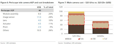
Samsung Camera BOM Reaches $83 in High End Smartphones

IFNews quotes UBS report with comparison of Samsung smartphone cameras over the years. The price of the camera grows steadily to $83 so far:


The perceived importance of the smartphone camera features rises among the consumers:

Tuesday, February 23, 2021

Reuters: Velodyne Founder and His Wife Fired for an Alleged Lack of Honesty

Reuters, BusinessWireVelodyne Lidar has removed its founder David Hall as chairman and his wife Marta Thoma Hall as marketing chief for a lack of honesty, a charge Marta Hall said the couple was not allowed to rebut in a board meeting she described as an “ambush.”

The investigation by the fully independent Audit Committee of the Company’s Board of Directors concluded that Mr. Hall and Ms. Hall each behaved inappropriately with regard to Board and Company processes, and failed to operate with respect, honesty, integrity, and candor in their dealings with Company officers and directors. Accordingly, the Board approved remedial actions including the removal of Mr. Hall as Chairman of the Board and the termination of Ms. Hall as an employee of the Company.

However, Marta Hall described the brief Friday board meeting at which she and her husband lost their jobs as a surprise, and added the SPAC, that took Velodyne public through a reverse merger last fall was trying to cut the Halls out of the decision-making process at Velodyne.

It was like an ambush,” she told Reuters in an interview. “We had no chance to defend ourselves.

David Hall is the largest shareholder of the company with a 35.43% stake as of Feb. 12, while Marta Hall owns a 3.74% stake.

Samsung Mass Produces 50MP Sensor with All-Pixel Split-PD AF

BusinessWire, BusinessWireSamsung introduces ISOCELL GN2, a 50MP sensor with 1.4μm pixels. The GN2 offers up to 100MP imaging, improved AF through Dual Pixel Pro technology, staggered HDR, and Smart ISO Pro. 

ISOCELL image sensors and its technologies have made vast improvements to deliver the quality and performance one would expect from top-tier prograde cameras,” said Duckhyun Chang, EVP of sensor business at Samsung. “Our new ISOCELL GN2 features Dual Pixel Pro, an innovative all-direction auto-focusing solution that elevates the agility to capture moments as they unfold. Adding on Smart ISO Pro and a variety of advanced pixel technologies, pictures from GN2 are more true-to-life than ever.

The 1/1.12-inch ISOCELL GN2 can simulate a larger 2.8μm-pixel with four-pixel-binning technology.

For those who appreciate more detail in photographs, the GN2 offers an option to take pictures in 100MP resolutions. In 100MP mode, the GN2 re-arranges the color pixels using an intelligent re-mosaic algorithm, creating three individual layers of 50MP frames in green, red and blue. These frames are then up-scaled and merged to produce a single 100MP resolution photograph.

The ISOCELL GN2 is Samsung’s first image sensor to offer Dual Pixel Pro, the company’s most advanced PDAF solution yet. By employing two photodiodes within every pixel of the image sensor, Dual Pixel Pro makes use of 100 million phase detecting agents for ultra-fast auto-focusing. In addition, the solution also offers all-direction focusing by splitting the pixels not only vertically, as with Dual Pixel, but also diagonally. This diagonal cut allows the focusing agents to better recognize the top and bottom of the frame, allowing the sensor to get in focus quickly even when there are no pattern changes in a horizontal direction. Low-light focusing and tracking of moving objects are improved as well, as every pixel of the sensor works as focusing agents.

The GN2 increases its DR with a staggered-HDR feature, a time-multiplexed HDR technology that uses rolling shutters over the same pixel arrays to capture multiple frames in short, middle, and long exposures. Staggered-HDR is able to reduce the energy consumption of a sensor by up to 24% when compared to the predecessor’s real-time HDR mode, contributing to improved energy efficiency of the overall system.

The GN2 also comes with Smart ISO and Smart ISO Pro. Smart ISO intelligently sets the sensor’s conversion gain, allowing the picture to be taken using an optimal ISO; low ISO for brighter outdoors or high for dimmer indoors. Unlike Smart ISO, which uses readouts from a single ISO per picture, Smart ISO Pro, which uses an intra-scene dual conversion gain (iDCG) solution, takes readouts from both high and low ISO to instantly create high dynamic range images with less motion-artifacts. In addition, in extreme low-light, Smart ISO Pro quickly takes and processes multiple frames in high ISO, raising the light sensitivity close to one-million ISOs and taking mobile night photography to greater heights.

The GN2 supports full-HD videos at 480fps or 4K at 120fps. The ISOCELL GN2 is currently in mass production.


Monday, February 22, 2021

Axcelis Ships Second 15MeV Implanter to "Leading CIS Foundry In Asia Pacific"

PRNewswire: Axcelis has shipped the second Purion XEmax high energy implanter to a leading CIS foundry in the Asia Pacific region.

Bill Bintz, EVP, Product Development explained, "Strong growth in the image sensor market continues to drive robust demand for high energy implant. The new Purion XEmax, combined with the popular Purion XE family of products, will extend Axcelis' market and technology leadership in this high growth market."

The new Purion XEmax high energy implanter was designed for image sensor applications. The enhanced beamline features multiple filtration systems to eliminate energetic metal contaminants which can otherwise result in compromised dark current and white pixel count levels. The new system is built on the industry leading Purion XE high energy implant platform and features Axcelis' patented Boost Technology, which delivers beam energies up to 15 MeV. Purion XEmax is delivering the most precise angle and overall process control to enable higher quality photodiode performance for next generation CIS devices.

First Image Sensor Startup in India

It came to my attention that there is a new image sensor startup in India - 3rdiTech, a spin-off from Indian Institute of Technology Delhi. The startup was founded by students of Albert Theuwissen's former student Mukul Sarkar who is Professor at IIT Delhi now. Few slides from the company's presentation:


Update: The last slide with sensor spec was removed at 2rdiTech request.

Sunday, February 21, 2021

Tower CIS Sales Represent 18% of Total Revenue

SeekingAlpha: Tower Semi's earnings call transcript gives some details about its image sensor sales. Only sensors for high end photography were separated, while other image sensors are mixed with other sales categories:

"Automotive was $180 million, which we serve with power ICs, power discretes, imaging and RF radar. Consumer, including computing, power management for home appliances and general accessories, and home-use security cameras was approximately $220 million. Industrial was approximately $100 million. Image sensors for high-end photography and medical applications, was at about $50 million.

Moving to our sensors and display business unit; first to discuss CMOS image sensors. In the past quarter with OPIX, we introduced a state-of-the-art indirect time-of-flight iToF imager with unparalleled performance and accuracy and sensitivity. Based on OPIX measurements, the sensor 17 accuracy are better, meaning higher level, higher performance than the two otherwise industry-leading iToF sensors in the market.

This sensor will enter volume production in the second quarter of this year. It is planned to be embedded in smartphones and other devices for face recognition and 3D imaging applications such as fast autofocus and artistic picture focused blurring effects. The sensor is based upon our unique pixel level stacking, state-of-the-art platform with the best in industry less than 2-micron electrical connection pitch.

During last year, we engaged in several programs of large x-ray sensors, some already having moved to production. Our differentiation in this market is in pixel performance, especially sensitivity and linearity and in yields.

For 300-millimeter, we are the only foundry to supply stitched sensors, in mass production. 300-millimeter tooling enables very high yields. And very importantly, a design advantage to manufacture a full, 21 centimeter, by 21 centimeter detector from one wafer and hence eliminating, the need for expensive wafer tiling.

Our next-generation industrial sensors on 300-millimeter, using our state-of-the-art global shutter pixels are also ramping into mass production. Our pixel size of 2.5 micron is the smallest in the world. We provide high-resolution sensors, with current maximum resolutions of 288 megapixels, with excellent sensitivity and shutter efficiency, for the display screening market.

We expect to see many of these new machine vision sensor products, based on our 65-nanometer, 300-millimeter platform, ramped to production this year. The industrial market continues to grow steadily. And we expect to see nice growth of these high-resolution sensors, tens of millions of dollars, at a high margin. The lifetime of such products is long, five to eight years.

The imaging area that for us was hit the hardest by COVID was dental X-ray. We are encouraged to see an initial increase in purchase orders and customer forecasts, now show second half of the year fully recovering, returning to pre-COVID run rates."

Zacks/SCR reports that image sensor sales represent about 18% of Tower revenue:

ZTE Announces Under-Display Structured Light 3D Camera

GizChina, IFNews: According to Ni Fei, president of ZTE’s mobile division and president of Nubia Technologies, ZTE will showcase the second generation of mass-produced under-screen camera technology at next week’s MWC Shanghai. It will debut under-screen 3D structured light camera.

We will show the world’s first under-screen 3D structured light technology! ZTE is the world’s first company to achieve true full-screen form, true 3D security, and human-machine interaction. It will provide a more wonderful selfie experience. It further lays a solid foundation for the future evolution of the smartphone form.  The world’s first demonstration of the second generation of mass-produced under-screen camera technology.


Meanwhile, ZTE Axon 20 5G under-display selfie camera takes one of the last spots in DxOMark ranking:

Saturday, February 20, 2021

ISSCC 2021: Sony SPAD for LiDAR Achieves 22% PDE at 905nm

Sony reports developing SPAD sensor for ist LiDAR with a record Photon Detection Efficiency (PDE) of 22% at 905nm, more than 15% at 940nm, and almost 30% at 850nm. It's also claimed to be the first stacked SPAD for LiDAR applications.

"Now, by leveraging Sony's technologies such as back-illuminated pixel structure, stacked configurations and Cu-Cu connections cultivated in the development of CMOS image sensors, and achieving the SPAD pixels and distance measuring processing circuitry on a single chip, Sony has succeeded in developing a compact yet high-resolution sensor.

This enables high-precision, high-speed measurement at 15-centimeter range resolutions up to a distance of 300 meters (When measuring an object with a height of 1 meter and reflectance of 10% using additive mode of 6 x 6 pixels (H x V) under cloudy daylight conditions.)"


Sony ISSCC 2021 presentation gives few more details about the new SPAD chip:

Friday, February 19, 2021

Sigma Scraps Next Generation Foveon Sensor Design Due to a Critical Flaw and Restarts from Scratch

ImagingResourceSigma publishes a statement about its full-frame Foveon X3 sensor development issues:

"In February 2020, we announced our decision to restart our plans for a full frame Foveon X3 sensor camera, beginning with the development of a new sensor technology. We have not been able to share any information regarding this project in the time since, and I would like to use this short message to provide an update about the situation.

As previously announced, we halted development of the project after the sensor we were working with could not go into mass production due to a critical flaw. As a result, we also terminated our contract with the sensor manufacturer with whom we had been collaborating. Further, we determined that the original sensor specifications would make it difficult to develop a product that will meet our and our customers’ high standards, and accordingly we decided to go back to the drawing board.

At present, we are fully engaged in research and development of the project, led by our head office, and are reviewing specifications to ensure that we will be able to satisfy the expectations placed on this project."

Sigma publishes a video with its CEO Kazuto Yamaki saying that due to the critical flaw in the design "we scrapped all the schematics and all the tooling and then re-started the project from the beginning":

AEye and Indie to Merge with SPACs at $2.4B and $1.4B Valuations Respectively

PRNewswireAEye and CF Finance Acquisition Corp. III, a special purpose acquisition company sponsored by Cantor Fitzgerald have entered into a merger agreement. The combined company will be called AEye Holdings, Inc. and is expected to be publicly listed on Nasdaq following the close of the transaction. Transaction values AEye at a pro-forma enterprise value of $2.0B and delivers up to $455M of gross proceeds to fully fund the company through profitability.


BusinessWire: Meanwhile, Indie Semi just saying that it will work on its own FMCW LiDAR, already enjoys almost $1.4B post-transaction valuation in another SPAC merger deal.

Thursday, February 18, 2021

ISSCC 2021: Sony 50.1MP Full-Frame Sensor with Sigma-Delta ADC and kTC Noise Reduction

Sony presents its full-frame 50.1MP sensor, apparently used in its new Alpha 1 high-end mirrorless camera:

"A High-Speed Back-Illuminated Stacked CMOS Image Sensor with Column-Parallel kT/C-Cancelling S&H and Delta-Sigma ADC"
by Chihiro Okada, Koushi Uemura, Luong Hung, Kouji Matsuura, Takashi Moue, Daisuke Yamazaki, Kazutoshi Kodama, Masafumi Okano, Takafumi Morikawa, Kazuyoshi Yamashita, Osamu Oka, Itai Shvartz, Golan Zeituni,  Ariel Benshem, Noam Eshel, Yoshiaki Inada.

"Sony presents a 50.1Mpixel, 4.16μm-pitch, back-illuminated stacked CIS with a pipelined column-parallel kT/C noise-cancelling sample-and-hold circuit and a 14b delta-sigma ADC achieving 1.18e-rms random noise at 250fps. The design splits the pixel signal line to lower the wiring load and increase the operation speed."

2021 International Image Sensor Workshop Final Call For Papers

International Image Sensor Workshop publishes the Final Call for Papers. The abstracts are due April 17, 2021.

Wednesday, February 17, 2021

ISSCC 2021: Albert Theuwissen's Plenary Talk

Albert Theuwissen's excellent Plenary video is available on Youtube again:


Update Feb. 22, 2021: An official ISSCC video is now posted in ISSCC channel.

ISSCC 2021: Nikon 17.84MP 1,000fps Sensor

Nikon presents is a stacked CMOS sensor with a total pixel count of approximately 17.84MP capable to operate at 1,000 fps speed at full resolution. The sensor supports HDR mode of 110 dB, and 4K x 4K video.

The 1-inch stacked sensor has 2.7um pixels. One of the available HDR modes supports 134dB DR at 60fps rate.

The pixel layer is split in 16 x 16 pixel blocks, or 264 x 264 blocks (4224 x 4224 pixels). It is possible to finely control the exposure of each of these blocks separately from the bottom logic chip.

ID Quantique Presentation about Image Sensor-Based Random Number Generator for Mobile Phones

ID Quantique publishes a webinar "Why Quantum Technology matters in mobile phone security":