Exosens - Photonis Infrared
R&D Engineer in Infrared & CMOS Image Sensor Grenoble, France Link
(Note: The listing at the link is in French)
R&D Engineer in Infrared & CMOS Image Sensor Grenoble, France Link
(Note: The listing at the link is in French)

|
OSRAM OS San Jose Sensor Characterization Engineer |
Boise, Idaho, USA |
|
|
DESY Instrument Scientist (Gamma Rays and UV) |
Hamburg, Germany |
|
|
Rockwell Automation EDGE – Support Engineer (Engineer in Training position) |
Mayfield Heights, Ohio, USA |
|
|
Jozef Stefan Institute Cherenkov-based PET Detector R&D, Postdoc |
Ljubljana, Slovenia |
|
|
onsemi Entry Level Analog Engineer |
Richardson, Texas, USA |
|
|
IDTechEx Sensors Analyst: Market Research & Consultancy |
London, England, UK |
|
|
Lockheed-Martin Corporation IR Camera Systems Engineer Early Career |
Santa Barbara, California, USA |
|
|
INSION GmbH Engineer Product Development Spectral Sensor Technology |
Obersulm, Germany |
 |
| Acuros GO 6 MP Camera Front |
 |
| Acuros GO 6 MP Camera Back |
 |
| Acuros GO 6 MP Camera Specification |
Sony Semiconductor Solutions - America
Automotive Image Sensor Field Applications Engineer Novi, Michigan, USA Link
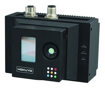
From: https://hokuyo-usa.com/resources/blog/pioneering-autonomous-capabilities-solid-state-3d-lidar
Autonomous technologies are proliferating across industries at breakneck speed. Various sectors, like manufacturing, agriculture, storage, freight, etc., are rushing to embrace robotics, automation, and self-driving capabilities.
At the helm of this autonomous transformation is LiDAR, the eyes that allow technologies to perceive and understand their surroundings. LiDAR is like a hawk scanning the landscape with sharp vision, giving clarity and insight into what stands before it. Additionally, research solidifies the claims of increasing LiDAR usage and anticipates that the global LiDAR market will reach 5.35 billion USD by 2030.
While spinning mechanical LiDAR sensors have paved the way, acting as the eyes of autonomous systems, they remain too bulky, delicate, and expensive for many real-world applications. However, new solid-state 3D LiDAR is here to change the game. These LiDARs pack thousands of tiny, durable laser beams onto a single chip to provide unmatched reliability and affordability.
How YLM-X001 3D LiDAR Range Sensor is Transforming Scanning Capabilities
The YLM-X001 outdoor-use 3D LiDAR by Hokuyo sets new standards with groundbreaking features. The range sensor has a small form factor with 119 (W) x 85 (D) x79 (H) dimensions, allowing it to become a part of any vehicle seamlessly. Additionally, despite the small size, it boasts a scanning range of 120° horizontally and 90° vertically. Therefore, it can scan a larger scene and provide data in real-time to avoid collisions with any object.
Furthermore, at the heart of this LiDAR range sensor is the Light Control Metasurface (LCM) technology patented and protected by Lumotive, Inc. This jointly developed light detection and ranging sensor works using this beam-steering technology. It uses the deflection angle of liquid crystals without relying on mechanical parts. This digital scanning technology combines a line light laser with VCSEL Laser and liquid crystal deflection, enabling LiDAR to perform efficient 3D object recognition with high resolution.
Also, the LCM not only eliminates mechanical components but also aids in reducing multipath interference and inter-sensor interference. Reduction of both interferences results in achieving a better level of stability in measurement that was previously unattainable using mechanical LiDARs.
The YLM-X001 3D LiDAR range sensors offer dynamic digital scanning, providing stable distance accuracy in multipath and LiDAR-to-LiDAR interference. It can measure the distance of stationary and repositioning objects in the moving direction and on the road surface via continuous and dynamic scanning.
Notable Features of YLM-X001
New and market-leading features are packed inside this LiDAR, making it a better choice than mechanical LiDARs.
Using 3D LiDAR in Real World Applications
The YLM-X001 finds its stride in various applications, making it an invaluable asset in robotics.
AGV/AMR Integration
Our 3D LiDAR sensors enhance AGV/AMR navigation and obstacle detection precision. They continuously scan the environment, providing real-time data, ideal for autonomous vehicles in dynamic environments.
Additionally, the fork trucks can utilize the capabilities of 3D LiDAR for accurate detection of container and pallet entrances. Plus, it can create path plans and ensure the accurate position of the forklift.
Service Robot Operations
Robots with the capabilities of 3D LiDAR will have an enhanced framework for avoiding obstacles and monitoring road surface conditions. Whether navigating complex indoor or outdoor spaces, these robots can adapt to changing conditions with unmatched accuracy.
Enhance Autonomous Mobility with Hokuyo YLM-X001 3D LiDAR
As industries embrace autonomous technology, the need for accurate range scanning sensors increases. Solid-state LiDARs offer a small form factor and precise measurements, becoming an ideal replacement for mechanical LiDARs.
Our team at Hokuyo is working relentlessly to help you achieve the pinnacle of autonomous mobility. We are developing high-end sensor solutions for a variety of autonomous applications. Our recent development, the YLM-X001 3D LiDAR range sensors, is here for accurate obstacle detection and continuous scanning.
Technical specifications of the YLM-X001 3D LiDAR range sensor: https://www.hokuyo-aut.jp/search/single.php?serial=247#drawing
In a paper titled "Silver telluride colloidal quantum dot infrared photodetectors and image sensors" Wang et al. from ICFO, ICREA, and Qurv Technologies (Spain) write:
Photodetectors that are sensitive in the shortwave-infrared (SWIR) range (1–2 µm) are of great interest for applications such as machine vision, autonomous driving and three-dimensional, night and adverse weather imaging, among others. Currently available technologies in the SWIR range rely on costly epitaxial semiconductors that are not monolithically integrated with complementary metal–oxide–semiconductor electronics. Solution-processed quantum dots can address this challenge by enabling low-cost manufacturing and simple monolithic integration on silicon in a back-end-of-line process. So far, colloidal quantum dot materials to access the SWIR regime are mostly based on lead sulfide and mercury telluride compounds, imposing major regulatory concerns for their deployment in consumer electronics due to the presence of toxic heavy metals. Here we report a new synthesis method for environmentally friendly silver telluride quantum dots and their application in high-performance SWIR photodetectors. The colloidal quantum dot photodetector stack employs materials compliant with the Restriction of Hazardous Substances directives and is sensitive in the spectral range from 350 nm to 1,600 nm. The room-temperature detectivity is of the order of 10^{12} Jones, the 3 dB bandwidth is in excess of 0.1 MHz and the linear dynamic range is over 118 dB. We also realize a monolithically integrated SWIR imager based on solution-processed, toxic-heavy-metal-free materials, thus paving the way for this technology to the consumer electronics market.Full paper (behind paywall): https://www.nature.com/articles/s41566-023-01345-3
Coverage in phys.org: https://phys.org/news/2024-01-toxic-quantum-dots-pave-cmos.html
Non-toxic quantum dots pave the way towards CMOS shortwave infrared image sensors for consumer electronics
Invisible to our eyes, shortwave infrared (SWIR) light can enable unprecedented reliability, function and performance in high-volume, computer vision first applications in service robotics, automotive and consumer electronics markets.
Image sensors with SWIR sensitivity can operate reliably under adverse conditions such as bright sunlight, fog, haze and smoke. Furthermore, the SWIR range provides eye-safe illumination sources and opens up the possibility of detecting material properties through molecular imaging.
Colloidal quantum dots (CQD)-based image sensor technology offers a promising technology platform to enable high-volume compatible image sensors in the SWIR.
CQDs, nanometric semiconductor crystals, are a solution-processed material platform that can be integrated with CMOS and enables access to the SWIR range. However, a fundamental roadblock exists in translating SWIR-sensitive quantum dots into key enabling technology for mass-market applications, as they often contain heavy metals like lead or mercury (IV-VI Pb, Hg-chalcogenide semiconductors).
These materials are subject to regulations by the Restriction of Hazardous Substances (RoHS), a European directive that regulates their use in commercial consumer electronic applications.
In a study published in Nature Photonics, ICFO researchers Yongjie Wang, Lucheng Peng, and Aditya Malla led by ICREA Prof. at ICFO Gerasimos Konstantatos, in collaboration with researchers Julien Schreier, Yu Bi, Andres Black, and Stijn Goossens, from Qurv, have reported on the development of high-performance infrared photodetectors and an SWIR image sensor operating at room temperature based on non-toxic colloidal quantum dots.
The study describes a new method for synthesizing size tunable, phosphine-free silver telluride (Ag2Te) quantum dots while preserving the advantageous properties of traditional heavy-metal counterparts, paving the way to the introduction of SWIR colloidal quantum dot technology in high-volume markets.
While investigating how to synthesize silver bismuth telluride (AgBiTe2) nanocrystals to extend the spectral coverage of the AsBiS2 technology to enhance the performance of photovoltaic devices, the researchers obtained silver telluride (Ag2Te) as a by-product.
This material showed a strong and tunable quantum-confined absorption akin to quantum dots. They realized its potential for SWIR photodetectors and image sensors and pivoted their efforts to achieve and control a new process to synthesize phosphine-free versions of silver telluride quantum dots, as phosphine was found to have a detrimental impact on the optoelectronic properties of the quantum dots relevant to photodetection.
In their new synthetic method, the team used different phosphine-free complexes such as a tellurium and silver precursors that led them to obtain quantum dots with well-controlled size distribution and excitonic peaks over a very broad range of the spectrum.
After fabricating and characterizing them, the newly synthesized quantum dots exhibited remarkable performances, with distinct excitonic peaks over 1,500nm—an unprecedented achievement compared to previous phosphine-based techniques for quantum dot fabrication.
The researchers then decided to implement the obtained phosphine-free quantum dots to fabricate a simple laboratory scale photodetector on the common standard ITO (Indium Tin Oxide)-coated glass substrate to characterize the devices and measure their properties.
"Those lab-scale devices are operated with shining light from the bottom. For CMOS integrated CQD stacks, light comes from the top, whereas the bottom part of the device is taken by the CMOS electronics," said Yongjie Wang, postdoc researcher at ICFO and first author of the study. "So, the first challenge we had to overcome was reverting the device setup. A process that in theory sounds simple, but in reality proved to be a challenging task."
Initially, the photodiode exhibited a low performance in sensing SWIR light, prompting a redesign that incorporated a buffer layer. This adjustment significantly enhanced the photodetector performance, resulting in a SWIR photodiode exhibiting a spectral range from 350nm to 1,600nm, a linear dynamic range exceeding 118 dB, a -3dB bandwidth surpassing 110 kHz and a room temperature detectivity of the order 10^{12} Jones.
"To the best of our knowledge, the photodiodes reported here have for the first time realized solution processed, non-toxic shortwave infrared photodiodes with figures of merit on par with other heavy-metal containing counterparts," Gerasimos Konstantatos, ICREA Prof. at ICFO and leading author of the study mentions.
"These results further support the fact that Ag2Te quantum dots emerge as a promising RoHS-compliant material for low-cost, high-performance SWIR photodetectors applications."
With the successful development of this heavy-metal-free quantum dot based photodetector, the researchers went further and teamed up with Qurv, an ICFO spin-off, to demonstrate its potential by constructing a SWIR image sensor as a case study.
The team integrated the new photodiode with a CMOS based read-out integrated circuit (ROIC) focal plane array (FPA) demonstrating for the first time a proof-of-concept, non-toxic, room temperature-operating SWIR quantum dot based image sensor.
The authors of the study tested the imager to prove its operation in the SWIR by taking several pictures of a target object. In particular, they were able to image the transmission of silicon wafers under the SWIR light as well as to visualize the content of plastic bottles that were opaque in the visible light range.
"Accessing the SWIR with a low-cost technology for consumer electronics will unleash the potential of this spectral range with a huge range of applications including improved vision systems for automotive industry (cars) enabling vision and driving under adverse weather conditions," says Gerasimos Konstantatos.
"SWIR band around 1.35–1.40 µm, can provide an eye-safe window, free of background light under day/night conditions, thus, further enabling long-range light detection and ranging (LiDAR), three-dimensional imaging for automotive, augmented reality and virtual reality applications."
Now the researchers want to increase the performance of photodiodes by engineering the stack of layers that comprise the photodetector device. They also want to explore new surface chemistries for the Ag2Te quantum dots to improve the performance and the thermal and environmental stability of the material on its way to the market.
|
Surrey Satellite Technology Ltd. Imager Electronics Engineer |
Guildford, Surrey, UK |
|
|
Booz Allen Hamilton Electro-Optical and Infrared Subject Matter Expert |
Crane, Indiana, USA |
|
|
SOITEC BU Director Mixed Signal |
Singapore or Grenoble, France |
|
|
Space Dynamics Laboratory Imaging Sensor and Detector Engineer |
Logan, Utah, USA |
|
|
University of Science and Technology of China Postdoctoral R&D of Monolithic Active Pixel Sensors |
Hefei, Anhui, China |
|
|
Nokia Silicon Photonics Design Engineer |
New York, New York, USA |
|
|
Nokia Silicon Photonics Design Summer Co-op |
New York, New York, USA |
|
|
Blue River Technology Camera Systems Engineer |
Santa Clara, California, USA |
|
|
Thorlabs – Imaging Systems Summer Intern |
Sterling, Virginia, USA |