Tuesday, September 29, 2015

Google Nexus 6P Features Large 12.3MP Sensor

The Verge, Phonearena, Androidpolice: Google announces Huawei-made Nexus 6P phone featuring a large 1/2.3-inch 12.3MP sensor with 1.55um pixels. The sensor is made by Sony. One of the trade-offs in such a large sensor size is a lack of optical image stabilization in Nexus 6P.

QIS Breakthrough Announced

EurekaAlert: Dartmouth's Thayer School of Engineering press release presents "an innovation that may usher in the next generation of light sensing technology with potential applications in scientific research and cellphone photography.

Thayer professor Eric Fossum -- the engineer and physicist who invented the CMOS image sensor used in nearly all cellphone and digital cameras, webcams, medical imaging and other applications -- joined with Thayer PhD candidate Jiaju Ma in developing pixels for the new Quanta Image Sensor (QIS).
"

"Their new sensor has the capability to significantly enhance low-light sensitivity. This is particularly important in applications such as "security cameras, astronomy, or life science imaging (like seeing how cells react under a microscope), where there's only just a few photons," says Fossum. "When we build an image sensor, we build a chip that is also sensitive to these photons. We were able to build a new kind of pixel with a sensitivity so high we could see one electron above all the background noise."

"The new pixels are considerably smaller than regular pixels since they are designed to sense only one photon, but many more are placed on the sensor to capture the same amount of total photons from the image. "We'd like to have 1 billion pixels on the sensor and we'll still keep the sensor the same size," says Ma."

"We deliberately wanted to invent it in way that is almost completely compatible with today's CMOS image sensor technology so it's easy for industry to adopt it," says Fossum. Engineering its size is a step in that direction.

"The question was how to build this in a current, commercially accessible, not-too-expensive CMOS process." he says. "You use all the tricks you can think of. Being able to measure one electron is fundamental from a scientific point of view and we were able to do it without a 'Manhattan Project'." Other challenges his group is working on are in reading out a billion pixels hundreds or thousands of time each second without dissipating too much heat, and also in creating images from all the data that is collected.

Monday, September 28, 2015

iPhone 6s Cameras Cost 7.7% of BOM

TechInsights' iPhone 6s teardown report reveals that its cameras cost is about 7.7% of the whole BOM, about the same proportion as in iPhone 6:


Business Insider gives an easier to grasp BOM chart, with camera being #4 most expensive component:


Update: IHS estimates the two cameras cost at $22.50:

Grand View on Image Sensor Market

PRNewswire: Grand View Research estimates global image sensor market at USD 8.81 billion in 2013. The market is expected to reach USD 12.03 billion by 2020, growing at a CAGR of 4.6% from 2014 to 2020.

Medical applications accounted for over 6.0% of overall image sensors market volume in 2013, and are expected to grow at a CAGR of 9.2% from 2014 to 2020. This growth is attributed to demand from minimally invasive procedures such as endoscopy.

CCD devices are particularly used in medical and scientific applications. The segment had a revenue share of over 12% in 2013, and is expected to grow at a CAGR of 1.3% from 2014 t0 2020.

North America image sensors market accounted for over 32% of the overall revenue in 2013. However, Asia Pacific is expected to outpace North America over the next six years. Countries such as India and China are expected to play a key role in regional growth.

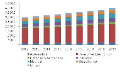
North America image sensor market revenue
by application, 2012-2020, (USD Million)

North America image sensor market was the largest regional industry in terms of revenue and is expected to grow at a CAGR of 3.7% from 2014 to 2020. This growth is attributed to stringent government regulations regarding driver and vehicle security.

North America was closely followed by Asia Pacific, which accounted for over 32% of the revenue share in 2013. Developing economies such as India, China, and Latin America countries are expected to majorly contribute to market growth

Europe image sensor market is also has a considerable revenue share of USD 2,006.8 million in 2013 is expected to be 2,503.1 million by 2020 growing at a CAGR of 3.2% from 2014 to 2020.

Saturday, September 26, 2015

DALSA CCD Foundry Business

I'm not sure if this is a fresh news, but Teledyne DALSA expands its foundry services to CCD process:

"Teledyne DALSA Semiconductor’s 150mm CCD process offers surface or buried channel operation at up to 15V with two or three layers of polysilicon and one, two or three layers of metal. A modular processing approach allows our foundry customers to adjust process parameters to meet the most demanding requirements for CTE (greater than 99.999%), charge storage capacity, and dark current (lower than 1nA/cm2). The base process uses 1X projection lithography with 2.5µm design rules, allowing die sizes of up to 100mm X 100mm. Where required, tighter alignment tolerances and smaller feature sizes can be obtained by using 5X lithography, using a mix and match or all-stepper approach. The maximum die size attainable with the stepper is 22mm X 22mm, but larger sensors can be fabricated using stitching."

Friday, September 25, 2015

Third Session of ToF Harvest Imaging Forum 2015

The first two sessions of the ToF Harvest Imaging Forum 2015 are sold out. On many many people requests, the speaker David STOPPA agreed to run a 3rd session on January 11-12, 2016 at the same location. Registration for the third session is open via the Harvest Imaging website.

SPI Color Night Vision Demos

SPI Corp publishes a dedicated page on its X27 color night vision camera with large number of Youtube videos, such as this one:


and another one:

Thursday, September 24, 2015

Omnivision Announces Sensor for Iris Recognition

PRNewswire: OmniVision announces the OV2281, a new PureCel sensor to implement a biometric security functionality mobile devices. The low-power, ultra-compact OV2281 leverages 1.12-micron pixel and optimized IR sensitivity. It enables reliable iris recognition for smartphones, tablets and notebooks, in both landscape and portrait orientations.

"With the convergence of digital identities, security concerns and mobile commerce, industry experts project that 13 billion biometric applications will be downloaded by 2.2 billion mobile users between 2014 and 2020, [according to Acuity Market Intelligence report]" said Archie de Guzman, staff product manager at OmniVision. "In this context, iris detection appears poised to become the next trend in biometric security for mobile devices. The OV2281 therefore enters the market as an extremely compelling solution by offering accurate horizontal or vertical iris detection in a compact and power-efficient package."

The 1/7.5-inch OV2281 PureCel sensor can record 1080p high-definition video at 60fps in both portrait and landscape orientation, thus supporting iris detection in either situation. When recording full-resolution 1920 x 1920 video at 30fps, the sensor requires just 120 mW. It also supports an ultra-low power mode that can reduce power consumption to approximately 25 mW. As a monochrome sensor, the OV2281 boasts exceptional IR sensitivity. This sensitivity allows it to produce clear and fully stable images in difficult low-light conditions.

The sensor fits into a 5.5 x 5.5 mm module with a z-height of less than 4.5 mm. The OV2281 is currently in volume production.

Olympus 16MP Stacked Global Shutter Sensor Presentation

Olympus presented its 16MP global shutter stacked sensor at Fraunhofer System Integration Technologies seminar in June 2015:

SPI Corp Presents Color Version of its Hyper Fidelity Intensified Sensor

SPI Corp. updates its Hyper Fidelity Intensified Sensor HFIS page and publishes a Youtube video of X27 sensor, said to be the color version of X26:

"COMING SOON: x27 COLOR TUBELESS NIGHT VISION Sensor, with full color day/night imaging capabilities, the video shown above was filmed at night with 1/4 moon conditions. Color Night vision Imaging performance and sensitivity has never been available until now."

Wednesday, September 23, 2015

0.22e- Read Noise Reported

IEEE Journal of the Electron Devices Society allows an early open access to the paper "Characterization of Quanta Image Sensor Pump-Gate Jots with Deep Sub-electron Read Noise" by Jiaju Ma, Dakota Starkey, Arun Rao, Kofi Odame, and Eric R. Fossum of Dartmouth College. The paper reports noise of the best pixel in the array of 0.22e-:


The average pixel noise was somewhat higher:


And here is the image lag measurements:

Grand View on Camera Module Market

BusinessWire: Grand View Research estimates the global camera module market size at USD 17.84 billion in 2014. Among the different electronic devices, smartphones and tablet PC is the major segment and is expected to acquire over 75% of the global market in terms of shipments in 2022. The industry is highly fragmented with no dominant player. LG-Innotek led the industry, and occupied a major share of the global market in 2014.

Tuesday, September 22, 2015

Black Silicon Presentation

Eric Mazur, Harward University Professor, Black Silicon inventor, and SiOnyx founder, publishes his presentation on Black Silicon properties and applications given at the 11th Conference on Lasers and Electro- Optics Pacific Rim (CLEO-PR 2015) in Busan, South Korea on 25 August 2015. Black Silicon is manufactured by high power laser treatment of the silicon surface and looks like this:


A TEM cross-sectional image reveals an interesting picture. It's scary to think that SiOnyx made image sensors out of this:

Imaging Companies in EETimes 60 Silicon Startups List

EETimes publishes its "Silicon 60: 2015's Startups to Watch" list. There are quite a few imaging companies there:
  • Geo Semiconductor Inc. (San Jose, Calif.) founded in 2009, is a fabless semiconductor company that designs video and geometry processing integrated circuits (ICs). Its chips have found use in consumer displays and projection systems and the company is moving into automotive and security applications.
  • Gpixel Inc. (Changchun, China) develops high-end CMOS image sensor solutions for industrial, medical and scientific applications. Founded in 2012, the company produces standard off-the-shelf image sensors, as well as customer-designed products. In 2014 Gpixel worked with foundry Tower Semiconductor Ltd. to produce a record-setting 150-Mpixel full-frame CMOS image sensor.
  • InVisage Technologies Inc. (Menlo Park, Calif.) is a fabless semiconductor company developing QuantumFilm, an imaging-sensing technology that it claims has superior performance to silicon. Its first product enables high-resolution images from handheld devices such as camera phones and PDAs. Founded in 2006, in 2015, InVisage opened its first high-volume manufacturing facility, QFAB3, in Hsinchu, Taiwan.
  • NeuroMem Inc. (Petaluma, Calif.) founded in October 2014 develops, markets and licenses neuromorphic circuits and sells chips, boards and development tools for pattern recognition and classification applications. Company is spin-off from General Vision Inc., developer of the CM1K neural network IC and the same technology is present in the Quark SE processor from Intel.
  • Softkinetic SA (Brussels, Belgium) founded in 2007 is a developer of sensor-to-software 3D gesture recognition systems. It has licensed its platform to Texas Instruments Inc. and Melexis SA.
  • TeraDeep Inc. (Santa Clara, Calif.) founded in December 2013 as spin off from Purdue University to focus on the design of mobile coprocessors and neural network hardware for the understanding of images and videos.
  • V-Nova Ltd. (London, England) founded in 2011 by Guido Meardi (CEO), Luca Rossato (chief scientist), Eric Achtmann (executive chairman) and Pierdavide Marcolongo (angel investor), to create a superior video codec. Perseus is the result and is being developed in an open innovation model with a business consortium that includes Broadcom, Encompass, Intel, Hitachi and Sky Italia.
  • Wavelens SA (Grenoble, France) is a CEA-Leti spinoff that was launched in November 2012. The company focuses on developing MEMS optical systems to integrate such autofocus, image stabilization and zoom.

TPSCo News

TowerJazz September 2015 newsletter updates on TowerJazz-Panasonic foundry progress:

"TPSCo has developed CIS production solutions with world leading quantum efficiencies, sub-blooming pixel charge saturation figures of merit, and dark current/white pixel performance due to our unique proprietary dual light pipe structure coupled with an ultra-deep photodiode structure. We offer 65nm CIS process solutions for pixel requirements from 1.12um to 6um and above pitch, in sensor sizes from VGA to full frame and above using 1D or 2D stitching technology. This includes full wafer 300mm sensors for X-ray applications. We are offering optimized pixel designs free of charge to qualified customers for fast sensor development. Additionally, we will offer a global shutter process with selected customer sampling in Q1 2016. Finally, we are now focusing on development of ultra-high QE sensors with a new light collecting technology. This technology will be ready for customer samples in 2017."

"[In Korea,] we have already started detailed discussions on CMOS image sensor (CIS) opportunities with several worldwide well-known surveillance and mobile companies who are interested in 65nm CIS technology on 300mm wafers. The state of the art pixel which is known as the best in the world is especially drawing customers’ attention."

Monday, September 21, 2015

How to Measure Blooming

Albert Theuwissen continues his series of posts on blooming measurements. Post #2 talks about difference between blooming and other effects that might behave in a similar way. Post #3 talks about vertical and horizontal blooming differences.

Sunday, September 20, 2015

ISORG Update

ARMdevices takes a video interview from Laurent Jamet demonstrating ISORG's printed image sensor at IDTechEx:

Saturday, September 19, 2015

Pinnacle to Offer Embedded HDR Tech for Licensing

PRWeb: Pinnacle Imaging Systems acquires the IP, products and trademarks developed by Unified Color Technologies with plans to offer its technology as embedded HDR solutions for digital still and video cameras.

With our technology embedded in next generation still and video cameras, system designers requiring improved video quality will be able to deliver the most accurate color and tonal rendition possible for real-time HDR capture,” said Alfred Zee, President & CEO of Pinnacle Imaging Systems.

HDR video capture is the new frontier for improving video quality and data capture for recognition. Currently, demand for HDR video is being driven from the top-down with digital content creators looking for HDR capabilities to be embedded into cameras and production equipment, and consumers seeking HDR-capable smart TV's and set top boxes. Eventually that demand will trickle down into consumer mobile devices over the next three to five years,” said Ron Tussy, Principal Analyst, The Imerge Group. “Embedded HDR tone mapping will not only improve the quality of video, but is also a critical underlying technology necessary to improve data for applications such as depth mapping and recognition in automotive ADAS as well as security/surveillance applications. Pinnacle Imaging Systems, with their proprietary IP, is the only provider of embedded HDR video that keeps all the color data intact and does so without a color shift.

Friday, September 18, 2015

Eye on Cars

Toshiba America VP of Image Sensor Business Unit Andrew Burt publishes a post on self-driven cars in his blog "Eye on Sensors." While mostly discussing legal and ethical issues of self-driving, the post also gives some statistics on automotive cameras:

"Vehicles may contain as many as 10 cameras when the age of self-driving cars arrives, and Strategy Analytics estimates that global shipments of automotive cameras will more than triple, reaching 102 million units by 2020 (see chart below)."

Photoneo Raises €2.1M Seed Money

IMV Europe: Bratislava, Slovakia-based Photoneo has secured a €2.1M seed investment. The investment was led by Prague-based venture capital firm Credo Ventures, with the participation of several co-investors including the investment arm of RSJ, one of the largest algorithmic trading companies in the world, co-founder of ESET Miroslav Trnka, Avast's co-founders Eduard Kucera and Pavel Baudiš, CEO of Ximea Max Larin, and founder of Finviz Juraj Duris.

Jan Zizka, CEO of Photoneo says: "The newly raised capital will allow our company to finish the image sensor chip thanks to which our camera will operate at full resolution at higher speeds. Additionally, we plan to strengthen our team on both technical and sales side to accommodate the large spectrum of use cases our potential customers are seeking to accommodate."

Update: The company says that its investment is one of the largest seed rounds recorded in Central Europe.

Infineon Provides ToF Camera for Kostal ADAS

Leopold Kostal is presenting a camera-based driver assistance system with Infineon ToF sensor inside. The system detects whether the driver is showing signs of drowsiness (nodding off) or is distracted. And the car instantly responds – with a vibrating seat or a warning tone, for instance. The less attentive the driver gets, the more attentive the car gets. In order to respond quickly and accurately, the assistance and the emergency braking systems can automatically activate in advance of a potential emergency.

For semi-autonomous or autonomous driving, the assistance system of the vehicle needs to know the state of the driver at all times,” says Frank Blaesing, Head of Innovation Management and Advanced Engineering at Kostal. “It needs to know if and how well the driver is informed about what’s happening on the road at that moment. This information is especially needed when the control over the vehicle needs to be turned back to the driver in a complex traffic situation.

By 2018, cars with the 3D camera system from Kostal will be running off the assembly line. The optical system is only 49 by 29 millimeters (about 2 by 1 inches) in size and is embedded into the dashboard: Through the steering wheel, it “looks” front-facing at the driver’s body and head. It records the exact head position and recognizes the blink of an eye even through glasses or sunglasses.

The heart of the camera system is the 3D ToF image sensor. At only 7 by 8 millimeters (.28 by .31 inches), it contains a 352 x 288 pixel array, intelligent control logic and a several ADCs. These convert the analog image data (distance and brightness) into digital data in less than a thousandth of a second. The robustness to ambient light irradiation is supported by the Suppression of Background Illumination (SBI) function. SBI is supplied by pmdtechnologies GmbH, the development partner of Infineon in the ToF technology and the 3D image sensor chips.

2016 BMW 7 Series Gesture Control

Autoevolution: One of the big new features in the new 2016 BMW 7 Series cars is a gesture control. "The system uses a 3D sensor installed in the roof lining of the car, next to the rearview mirror. It recognizes the hand gestures of the driver, as long as he keeps his hand between the steering wheel, dash and the gearshift lever. The system works best if you use gestures close to the dash and in front of the iDrive screen."

BMW video tutorial shows its operation:

Thursday, September 17, 2015

Photoneo 3D Multi-Image Sensing

Slovakia-based 3D camera startup Photoneo announces its ToF PhoXi Cam:

"We are changing the industry and are working hard to make the impossible a reality. Our patent pending technology embedded into the PhoXi Cam can deliver the high quality outputs of the structured light systems like PhoXi Scan with the speed of Time of Flight systems.

Based on our revolutionary sensor technology, we are able to capture the high-resolution 3D data with a single frame of the camera. We call it the Multi-Image sensing and it is based on a massive parallelism on a level of photons. In collaboration with our projection unit, it basically freezes objects in space and deliver a motion-blur free 3D reconstruction. It is suitable for all dynamic applications (alongside of all static ones).

This level of performance is possible due to our custom-design smart CMOS sensor. We hope, that our camera will help to shape the new wave of industry automation. To serve as a vision platform for new autonomous systems aware of their surroundings.
"

It appears that Germany-based Ximea was somehow involved in PhoXi Cam design.


Photoneo's only published patent application WO2015132726 "Method and Apparatus for Superpixel Modulation" by KOVACOVSKY Tomas, MALY Michal, and ZIZKA Jan has 105 pages and describes a modulated structured light image sensor, rather than the ToF one. The application presents an array of superpixels, each of them being a group of 3 x 3 pixels. Each pixel in the group get orthogonal demodulation signals:

Sony PDAF Patent Application

Imaging Resource noticed Sony PDAF patent application published in Japanese language Egami blog. The application presents an asymmetrical microlens covering two neighboring pixels:

Rambus Presents Eye Tracking Application for its Lensless Sensor

Rambus publishes a Youtube video showing eye tracking use case for its LSS image sensor, among few other use cases:

Wednesday, September 16, 2015

Hamamatsu ToF Sensor Principle Revealed

So far, Hamamatsu ToF image sensor operation principles have not been presented to the broad public. University of Siegen, Germany, MSc Thesis "Analysis of a pulse-based ToF camera for automotive application" by Simon Theiß fills this gap. The work is based on Hamamatsu S11963-01CR sensor:

4K Resolution, Extended Color Gamut Space Find Their Way to Endoscopes

Sony, Olympus, and their medical joint venture - Sony Olympus Medical Solutions Inc. - announce that their jointly developed 4K surgical endoscopy system will be commercialized since early October 2015. Sony Olympus Medical Solutions has brought together the core technologies and expertise of Sony (image sensors, image and signal processing, optical transmission, 4K imaging) and Olympus (medical products R&D, deep understanding of the needs of the medical community) and combined them to create a powerful technological base and image processing system for medical devices.

Sony contributed its technology and expertise in 4K and digital imaging. For the 4K camera head, Sony provided its 4K Exmor R CMOS image sensor, image and signal processing technologies, and miniaturization technologies, which - taken together - make for very high image clarity and advanced functionality. In addition, Sony's 4K image transmission technologies made possible the nearly latent-free delivery of 4K visuals from the endoscope to the monitor.

Tuesday, September 15, 2015

ST ToF-Assisted AF Adopted in Many Smartphones

After LG G3 smartphone has presented ST ToF sensor-assisted AF last year and G4 is following its path this year, there are few more smartphone makers adopting ST ToF solution. One of them is the recently announced Oppo R7 Plus: "With a laser focus technology to quickly capture the focal point within 0.3 seconds, a RGBW sensor that is able to shoot high-clarity photos in low-light environments <..> to capture <..> sports events."


Another recent smartphone with ST VL6180 ToF sensor is OnePlus 2: "The 2015 flagship model, OnePlus 2, relies on ST sensors for its superior camera system performance that includes an ultra-fast 0.2s “human-eye” -grade focus time and advanced optical anti-shake technology that delivers a 20% improvement in effective image resolution, as well as a 55% reduction in power consumption compared with standard optical anti-shake mobile-camera systems."


Asus Zenphone 2 Laser too features ToF sensor AF: "The brand-new laser-autofocus feature greatly reduces blurring and enhances image stabilization..."


There are few more models from LG and Asus, as well as Lenovo Vibe Shot, and Meizu MX5. There is even a rumor that the next generation Google Nexus will have the ToF AF too:

Talk on Hyperspectral Imaging Applications

SpectroNet publishes a video presentation "Multi/Hyper-Spectral Imaging Applications" by Vivek Sharma - KU Leuven / IMEC:

Monday, September 14, 2015

Omnivision Announces Two Versions of 8MP Sensor for Smartphones

PRNewswire: OmniVision announces the OV8856, a 1/4-inch 8MP, 1.12um pixel PureCel sensor for mainstream mobile devices.

"The global market for 8-megapixel sensors is booming, with analysts expecting over one billion in annual unit sales by 20171. A vast number of mainstream mobile handsets are already using 8-megapixel cameras for their rear-facing cameras. Looking forward, industry observers expect a strong trend toward an ever-increasing number of mobile handsets with their former 1/4-inch 5-megapixel cameras upgraded to 1/4-inch 8-megapixel cameras2," said Arun Jayaseelan, product marketing manager at OmniVision. "The capabilities and compactness of the OV8856 address the increasing consumer demand for higher resolution and more advanced features in mobile front- and rear-facing cameras."

The OV8856 captures full-resolution 8MP images and video at 30fps, and 1080p video at 60fps. The sensor also supports interlaced HDR (iHDR) for HDR video. The OV8856 is said to be one of the smallest 8MP sensors in the market today, and is approximately 15 percent smaller than OmniVision's previous generation OV8858 image sensor. It can fit into a 6.5 mm x 6.5 mm fixed focus module with a z-height of approximately 4 mm.

OmniVision also announces the OV8855, a variation of the OV8856 with PDAF. Both sensors are currently available for sampling, and are expected to enter volume production in the fourth quarter of 2015.

Sunday, September 13, 2015

NHK Presents 8K HDR System

While Canon is first to unveil its plans to commercialize the first affordable 8K Cinema camera, NHK is already talking about 8K HDR system at IBC 2015 being held these days in Amsterdam, the Netherlands.