Tuesday, May 31, 2022

SmartSens Goes Public on Shanghai Stock Exchange

From PRNewsWire:


SHANGHAI, May 23, 2022 /PRNewswire/ -- On May 20, 2022, SmartSens was officially listed on the Science and Technology Innovation Board of the Shanghai Stock Exchange (Stock Code: 688213). On the first day of trading, SmartSens shares surged by 79.82%, with a total market value of 22.66 billion yuan.


SmartSens Technology (Shanghai) Co., Ltd. (Stock Code: 688213) is a high-performance CMOS image sensor (CIS) chip design company. It is headquartered in Shanghai and has research centers in many cities around the world.

SmartSens has been dedicated to pushing forward the frontier of imaging technology and growing in popularity among customers since it was established. SmartSens' CMOS image sensors provide advanced imaging solutions for a broad range of areas such as surveillance, machine vision, automotive and cellphone cameras.

SmartSens is committed to continuous innovation of products and fueling growth in numerous industries by delivering a more comprehensive portfolio of image sensors.

Monday, May 30, 2022

Preprint on unconventional cameras for automotive applications

From arXiv.org --- You Li et al. write:

Autonomous vehicles rely on perception systems to understand their surroundings for further navigation missions. Cameras are essential for perception systems due to the advantages of object detection and recognition provided by modern computer vision algorithms, comparing to other sensors, such as LiDARs and radars. However, limited by its inherent imaging principle, a standard RGB camera may perform poorly in a variety of adverse scenarios, including but not limited to: low illumination, high contrast, bad weather such as fog/rain/snow, etc. Meanwhile, estimating the 3D information from the 2D image detection is generally more difficult when compared to LiDARs or radars. Several new sensing technologies have emerged in recent years to address the limitations of conventional RGB cameras. In this paper, we review the principles of four novel image sensors: infrared cameras, range-gated cameras, polarization cameras, and event cameras. Their comparative advantages, existing or potential applications, and corresponding data processing algorithms are all presented in a systematic manner. We expect that this study will assist practitioners in the autonomous driving society with new perspectives and insights.


Friday, May 27, 2022

Single Photon Workshop 2022 - Call for Papers

After a short hiatus, Single Photon Workshop will be held in person from October 31 to November 4, 2022 at the Korea Institute of Science and Technology (KIST) in Seoul, South Korea.


SPW 2022 is the tenth and latest installment in a series of biennial workshops on single-photon technologies and applications. After one-year delay due to COVID-19, SPW 2022 is intended to bring together again a broad range of people with interests in single-photon sources, single-photon detectors, photonic quantum metrology, and their applications such as quantum information processing. Researchers from universities, industry, and government will present their latest developments in single-photon devices and methods with a view toward improved performance and new application areas. It will be an exciting opportunity for those interested in single-photon technologies to learn about the state-of-the-art and to foster continuing partnerships with others seeking to advance the capabilities of such technologies.

1-page abstract submissions are now being accepted on various topics (see table below). Submission period is from Apr 25 - July 1, 2022.


The KIST campus is located in the northeast side of Seoul and can be easily reached by subway from anywhere in Seoul and near Seoul. The presentation room would be Johnson Auditorium in Building A1 with a seating capacity of 420 people. For poster presentation and exhibition, an open space in the 1st floor in L3 would be reserved.

Visit http://spw2022.org/ for more information.

Thursday, May 26, 2022

PreAct and Espros working on new lidar solutions

From optics.org news:

PreAct Technologies, an Oregon-based developer of near-field flash lidar technology and Espros Photonics, Sargans, Switzerland, a firm producing time-of flight chips and 3D cameras, have announced a collaboration agreement to develop new flash lidar technologies for specific use cases in automotive, trucking, industrial automation and robotics.

The collaboration combines the dynamic abilities of PreAct’s software-definable flash lidar and the “ultra-ambient-light-robust time-of-flight technology” from Espros with the aim of creating what the partners call “next-generation near-field sensing solutions”.

Paul Drysch, CEO and co-founder of PreAct Technologies, commented, “Our goal is to provide high performance, software-definable sensors to meet the needs of customers across various industries. Looking to the future, vehicles across all industries will be software-defined, and our flash lidar solutions are built to support that infrastructure from the beginning.”


The automotive and trucking industries continue to rapidly integrate ADAS and self-driving capabilities into vehicles, and as the US NHTSA has just announced the requirement for human controls in fully automated vehicles, the need for ultra-precise, high performance sensors is paramount to ensuring safe autonomous driving.

The sensors created by PreAct and Espros are expected to address significant ADAS and self-driving features – such as traffic sign recognition, curb detection, night vision and pedestrian detection – with the highest frame rates and resolution of any sensor on the market, the partners state.


In addition to providing solutions for automotive and trucking, the partnership will also address the expanding robotics industry. According to a market report published by Allied Market Research, the global industrial robotics market size is expected to reach $116.8 billion by 2030.

The flash lidar technologies solutions will also enable a wide range of robotics and automation applications including QR code scanning, obstacle avoidance and gesture recognition.

Beat DeCoi, President and CEO of Espros, commented, “We have plans to demonstrate the capabilities of our 3D chipsets with PreAct’s hardware and software. By combining our best in class TOF chips with PreAct’s innovation and drive, we will see great results with clients benefiting from this partnership.”

Link: https://optics.org/news/13/3/41

Tuesday, May 24, 2022

Veoneer and BMW agreement on next-gen automotive vision systems

Veoneer to supply Cameras to BMW Group's Next Generation Vision System for Automated Driving

Stockholm, Sweden, May 18, 2022: The automotive technology company Veoneer has signed an agreement to equip BMW Group vehicles with camera heads for their next generation vision system for Automated Driving. The camera heads support the cooperation between BMW Group, Qualcomm Technologies, and Arriver™ which was announced in March this year.

The high definition 8 MP camera, mounted behind the rear-view mirror, monitors the forward path of the vehicle to provide reliable and accurate information to the vehicle control system.  

In BMW's next generation of Automated Driving Systems, BMW Group's current AD stack is combined with Arriver's Vision Perception and NCAP Drive Policy products on Qualcomm Technologies' system-on-chip, with the goal of designing best-in-class Automated Driving functions spanning NCAP, Level 2 and Level 3. Veoneer's camera heads are adapted to the current trend of a centralized and scalable software architecture and will be an essential part of the sensor set-up required for the next generation AD platform.

"We are excited to be part of the development of the next generation vision systems, planned to enter the market in 2025", says Jacob Svanberg, CEO of Veoneer. "This award with camera heads to the 5th generation vision system is another proof point that Veoneer remains at the forefront of providing safe, collaborative driving solutions."

Veoneer is an automotive technology company. As a world leader in active safety and restraint control systems, Veoneer is focused on delivering innovative, best-in-class products and solutions. Our purpose is to create trust in mobility. Veoneer is a Tier-1 hardware supplier and system integrator with products being part of more than 125 scheduled vehicle launches for 2022.  Headquartered in Stockholm, Sweden, Veoneer has 6,100 employees in 11 countries. The Company is building on a heritage of close to 70 years of automotive safety development. 

https://www.veoneer.com/en/press-releases?page=/press/perma/2022030

Monday, May 23, 2022

ams OSRAM VCSELs in Melexis' in-cabin monitoring solution

ams OSRAM VCSEL illuminator brings benefits of integrated eye safety to Melexis automotive in-cabin monitoring solution

Premstaetten, Austria (11 May, 2022) – ams OSRAM (SIX: AMS), a global leader in optical solutions, announces that it is supplying a high-performance infrared laser flood illuminator for the latest automotive indirect Time-of-Flight (iToF) demonstrator from Melexis.

The ams OSRAM vertical-cavity surface-emitting laser (VCSEL) flood illuminator from the TARA2000-AUT family has been chosen for the new, improved version of the EVK75027 iToF sensing kit because it features an integrated eye safety interlock. This provides for a more compact, more reliable and faster system implementation than other VCSEL flood illuminators that require an external photodiode and processing circuitry.

The Melexis evaluation kit demonstrates the combined capabilities of the new ams OSRAM 940nm VCSEL flood illuminator in combination with an interface board and a processor board and the MLX75027 iToF sensor. The evaluation kit provides a complete hardware implementation of iToF depth sensing on which automotive OEMs can run software for cabin monitoring functions such as occupant detection and gesture sensing.


More reliable operation, faster detection of eye safety risks

The new ams OSRAM VCSEL with integrated eye safety interlock is implemented directly on the micro-lens array of the VCSEL module, and detects any cracks or apertures that can cause an eye safety risk. Earlier automotive implementations of iToF sensing have used VCSEL illuminators that require an external photodiode, a fault-prone, indirect method of providing the eye safety interlock function.

The read-out circuit requires no additional components other than an AND gate or a MOSFET. This produces almost instant (<1µs) reactions to fault conditions. A lower component count also reduces the bill-of-materials cost compared to photodiode-based systems. By eliminating the use of an external photodiode, the eye safety interlock eliminates the false signals created by objects such as a passenger’s hand obscuring the camera module.

“Automotive OEMs are continually looking for ways to simplify system designs and reduce component count. By integrating an eye safety interlock into the VCSEL illuminator module, ams OSRAM has found a new way to bring value to automotive customers. Not only will it reduce component count, but also increase reliability while offering the very highest levels of optical performance,” said Firat Sarialtun, Global Segment Manager for In-Cabin Sensing at ams OSRAM.

“With the EVK75027, Melexis has gone beyond the provision of a stand-alone iToF sensor to offer automotive customers a high-performance platform for 3D in-cabin sensing. We are pleased to be able to improve the value of the EVK75027 by now offering the option of a more integrated VCSEL flood illuminator on the kit’s illuminator board,” said Gualtiero Bagnuoli, Marketing manager Optical Sensors.

The EVK75027 evaluation kit with ams OSRAM illumination board can be ordered from authorized distributors of Melexis products (https://www.melexis.com/en/product/EVK75027/Evaluation-Kit-VGA-ToF-Sensor).

There is also a white paper on the new illumination board for the EVK75027, describing the benefits of implementing an iToF system with a VCSEL flood illuminator that includes an eye safety interlock. The white paper can be downloaded here: https://www.melexis.com/Eye-safe-IR-illumination-for-3D-TOF

Article: https://ams-osram.com/news/press-releases/melexis-eye-safety-itof

Friday, May 20, 2022

"End-to-end" design of computational cameras

A team from MIT Media Lab has posted a new arXiv preprint titled "Physics vs. Learned Priors: Rethinking Camera and Algorithm Design for Task-Specific Imaging".

Abstract: Cameras were originally designed using physics-based heuristics to capture aesthetic images. In recent years, there has been a transformation in camera design from being purely physics-driven to increasingly data-driven and task-specific. In this paper, we present a framework to understand the building blocks of this nascent field of end-to-end design of camera hardware and algorithms. As part of this framework, we show how methods that exploit both physics and data have become prevalent in imaging and computer vision, underscoring a key trend that will continue to dominate the future of task-specific camera design. Finally, we share current barriers to progress in end-to-end design, and hypothesize how these barriers can be overcome.


Thursday, May 19, 2022

Advanced Navigation Acquires Vai Photonics

Advanced Navigation, one of the world’s most ambitious innovators in AI robotics, and navigation technology has today announced the acquisition of Vai Photonics, a spin-out from The Australian National University (ANU) developing patented photonic sensors for precision navigation. 
Vai Photonics share a similar vision to provide technology to drive the autonomy revolution and will join Advanced Navigation to commercialise their research into exciting autonomous and robotic applications across land, air, sea and space.

“The technology Vai Photonics is developing will be of huge importance to the emerging autonomy revolution. The synergies, shared vision and collaborative potential we see between Vai Photonics and Advanced Navigation will enable us to be at the absolute forefront of robotic and autonomy driven technologies,” said Xavier Orr, CEO and co-founder of Advanced Navigation. 

“Photonic technology will be critical to the overall success, safety and reliability of these new systems. We look forward to sharing the next generation of autonomous navigation and robotic solutions with the global community.”

James Spollard, CTO and co-founder of Vai Photonics detailed the technology “Precision navigation when GPS is unavailable or unreliable is a major challenge in the development of autonomous systems. Our emerging photonic sensing technology will enable positioning and navigation that is orders of magnitude more stable and precise than existing solutions in these environments.

“By combining laser interferometry and electro-optics with advanced signal processing algorithms and real-time software, we can measure how fast a vehicle is moving in three dimensions. As a result, we can accurately measure how the vehicle is moving through the environment, and from this infer where the vehicle is located with great precision.”

The technology, which has been in development for over 15 years at ANU, will solve complex autonomy challenges across aerospace, automotive, weather, space exploration as well as railways and logistics.

Aircraft with an electric vertical takeoff and landing system such as flying taxis will greatly benefit from this technology. Landing and takeoff are often considered the most dangerous and expensive part of a flight route. Vai Photonics sensors will provide safe and reliable autonomous takeoff and landings under all conditions. 

Space travel and exploration is fraught with risks, vast complexity and enormous cost. This technology will bring massive benefits to space missions, helping to cement Advanced Navigation as the gold-standard for space-qualified navigation systems for space exploration. 

Professor Brian Schmidt, Vice-Chancellor of the Australian National University said “Vai Photonics is another great ANU example of how you take fundamental research – the type of thinking that pushes the boundaries of what we know – and turn it into products and technologies that power our lives.

“The work that underpins Vai Photonics’ advanced autonomous navigation systems stems from the search for elusive gravitational waves – ripples in space and time caused by massive cosmic events like black holes colliding.

From: https://www.suasnews.com/2022/05/shaping-the-future-of-photonic-sensing-advanced-navigation-acquires-vai-photonics/?amp 

Friday, May 13, 2022

Prof. Eric Fossum's interview at LDV vision summit 2018

Eric Fossum & Evan Nisselson Discussing The Evolution, Present & Future of Image Sensors

Eric Fossum is the inventor of the CMOS image sensor “camera-on-a-chip” used in billions of cameras, from smartphones to web cameras to pill cameras and many other applications. He is a solid-state image sensor device physicist and engineer, and his career has included academic and government research, and entrepreneurial leadership. He is currently a Professor with the Thayer School of Engineering at Dartmouth in Hanover, New Hampshire where he teaches, performs research on the Quanta Image Sensor (QIS), and directs the School’s Ph.D. Innovation Program. Eric and Evan discussed the evolution of image sensors, challenges and future opportunities.


More about LDV vision summit 2022: https://www.ldv.co/visionsummit

Organized by LDV Capital https://www.ldv.co/


[An earlier version of this post incorrectly mentioned this interview is from the 2022 summit. This was in fact from 2018. --AI]

Thursday, May 12, 2022

Photonics magazine article on Pi Imaging SPAD array

Photonics magazine has a new article about Pi Imaging Technology's high resolution SPAD sensor array; some excerpts below.


As the performance capabilities and sophistication of these detectors have expanded, so too have their value and impact in applications ranging from astronomy to the life sciences.

As their name implies, single-photon avalanche diodes (SPADs) detect single particles of light, and they do so with picosecond precision. Single-pixel SPADs have found wide use in astronomy, flow cytometry, fluorescence lifetime imaging microscopy (FLIM), particle sizing, quantum computing, quantum key distribution, and single- molecule detection. Over the last 10 years, however, SPAD technology has evolved through the use of standard complementary metal-oxide-semiconductor (CMOS) technology. This paved the way for arrays and image sensor architectures that could increase the number of SPAD pixels in a compact and scalable way. 

Compared to single-pixel SPADs, arrays offer improved spatial resolution and signal-to-noise ratio (SNR). In confocal microscopy applications, for example, each pixel in an array acts as a virtual small pinhole with good lateral and axial resolution, while multiple pixels collect the signal of a virtual large pinhole.


Challenges: 

Early SPADs produced as single-point detectors in custom processes offered poor scalability. In 2003, researchers started using standard CMOS technology to build SPAD arrays. This change in design and production platform opened up the possibility to reliably produce high-pixel-count SPAD detectors, as well as invent and integrate new pixel circuity for quenching and recharging, time tagging, and photon-counting functions. Data handling in these devices ranged from simple SPAD pulse outputting to full digital signal processing.
Close collaboration between SPAD developers and CMOS fabs, however, has helped SPAD technology overcome many of its sensitivity and noise challenges by adding SPAD-specific layers into the semiconductor process flow, design innovations in SPAD guard rings, and enhanced fill factors made possible by microlenses. 


Applications:

Research on SPADs also focused on the technology’s potential in biomedical applications, such as Raman spectroscopy, FLIM, and positron emission tomography (PET).

FLIM [fluorescence lifetime imaging microscopy] benefits from the use of SPAD arrays, which allow faster imaging speeds by increasing the sustainable count rate via pixel parallelization. SPAD image sensors enhanced with time-gating functions can further expand the implementation of FLIM to nonconfocal microscopic modalities and thus establish FLIM in a broader range of potential applications, such as spatial multiplexed applications in a variety of biological disciplines including genomics, proteomics, and other “-omics” fields.

One additional application where SPAD technology is forging performance enhancements is high-speed imaging, in which image sensors typically suffer from low SNR. The shorter integration times in these operations lead to lower photon collection and pixel blur, while the faster readout speeds increase noise in the collected image. SPAD image sensors fully eliminate this noise to offer Poisson-maximized SNR. 


A signal-to-noise ratio (SNR) comparison between a SPAD with 50% sensitivity and a typical photodiode with 80% sensitivity, both with equivalent readout noise of 10 e− (representative only for high-speed readout mode). Courtesy of Pi Imaging Technology.


A demonstration of SNR differences between a typical photodiode with 80% sensitivity and 10 e− signal (representative only for high-speed readout mode) equivalent readout noise (top) and a SPAD with 50% sensitivity (bottom), both at 10 impinging photons average. Courtesy of Pi Imaging Technology.


A SPAD array system implementation for image-scanning microscopy applications.


A fluorescence lifetime imaging microscopy (FLIM) image of mouse embryo tissue recorded with a single-photon-counting confocal microscope. Courtesy of PicoQuant.


About Pi Imaging:

Pi Imaging Technology is fundamentally changing the way we detect light. We do that by creating photon-counting arrays with the highest sensitivity and lowest noise.

We enable our partners to introduce innovative products. The end-users of these products perform cutting-edge science, develop better products and services in life science and quantum information.

Pi Imaging Technology bases its technology on 7 years of dedicated work at TU Delft and EPFL and 6 patent applications. The core of it is a single-photon avalanche diode (SPAD) designed in standard semiconductor technology. This enables our photon-counting arrays to have an unlimited number of pixels and adaptable architectures.


Full article here: https://www.photonics.com/Articles/Single-Photon_Avalanche_Diodes_Sharpen_Spatial/p5/vo211/i1358/a67902

Wednesday, May 11, 2022

Newsight CMOS ToF sensor release

NESS ZIONA, Israel, Feb. 14, 2022 /PRNewswire/ -- Newsight Imaging - a leading semiconductor innovator developing machine vision sensors, spectral vision chips, and systems - announced today the upcoming release of the NSI9000 one-chip (non-stacked) CMOS image sensor solution for depth imaging. The new chip is equipped with 491,520 depth 5x5 micron pixels (1024x480) (almost 5X more than its closest competitor), global shutter (with up to 132 fps on full resolution), and an estimated depth accuracy of less than 1% of the distance. The sensor is designed for an optimal distance of 0-200 meters. The new chip offers new capabilities at a competitive price to significant growth markets for LiDAR systems, automotive ADAS, Metaverse AR/VR applications, Industry 4.0, and smart city/IOT, including smart traffic 3D vision systems.

The sensor is a result of five years of collaborative innovation by Newsight and its partners such as Fraunhofer and Tower-Jazz. The product offers unique features, including:

Newsight's patented enhanced Time-Of-Flight (eTOF) technology that is well demonstrated on the currently available NSI1000 sensor chip. This technology enables maximal flexibility using multi-sets of configurations, in-pixel accumulation, and a novel depth calculating method that does not require heavy calculations and expensive MCU.
Event aware unique circuit, which was developed as part of the Israeli smart imaging consortium (https://www.smartimagingiia.com/). The solution enables event driven imaging, while a unique circuit attached to each pixel makes it possible to broadcast only lines with pixels that were changed from a previous frame. This feature is specifically designed for smart-city enabled cameras and smart traffic solutions.
Multi-triangulation: a unique solution for industry 4.0 applications and measurement devices of 480 ultra-accurate depth points, down to micron accuracy for close 3D inspection of production rail objects.
Built in fusion, allowing the sensor to extract a full resolution B/W image together with a depth image from the same frame data, and making image and depth fusion trivial for systems developers.
Chip design using a standard CMOS image sensor process, with only two system power source requirements (1.8V, 3.3V), making it a low-power, easy to integrate, and affordable solution for mass markets.


Eyal Yatskan, Newsight CTO and Co-founder, noted: "Newsight has implemented significant, proven, and innovative ideas in this sensor and accelerated the capabilities of the solution to match the high-end requirements of our customers' target applications. Newsight believes that such advanced solutions can be offered at affordable prices for building high volume best ROI depth imaging products."

Newsight will be offering a complete demo system using its eTOF Lidar reference design starting August 2022.

https://www.prnewswire.com/il/news-releases/newsight-imaging-to-release-the-nsi9000-an-affordable-cmos-image-sensor-providing-advanced-features-for-depth-sensing-and-lidar-applications-with-built-in-etof-technology-and-event-detection-capabilities-301481772.html

Tuesday, May 10, 2022

Apple iPhone LiDAR applications

Polycam makes apps that leverage the new lidar sensor on Apple's latest iPhone and iPad models.

Their website presents a gallery of objects scanned with their app: https://poly.cam/explore


Original press release about Polycam's new app:

Polycam launches a 3D scanning app for the new iPhone 12 Pro models with a LiDAR sensor. The app allows users to rapidly create high quality, color 3D scans that can be used for 3D visualization and more. Because the scans are dimensionally accurate, they can be used to take measurements of virtually anything in the scan at once, rapidly speeding up workflows for many professionals such as architects and 3D designers. What is perhaps most impressive about Polycam is the speed -- scans which would have taken hours to process on a desktop without a LiDAR device can now be processed in seconds directly on an iPhone. 

As Chris Heinrich, the CEO of Polycam, puts it: "I've worked for years on 3D scanning with more conventional hardware, and what you can do on these LiDAR devices is literally 100x faster than what was possible before".

3D capture is a valuable tool for many industries, and Polycam is already seeing enthusiastic usage from architects, archaeologists, movie set designers and more, via an iPad Pro version that launched earlier this year. With the launch of the iPhone version, Heinrich expects to see adoption from many more users across a wider range of verticals. "Just as smartphones dramatically expanded the reach of photo and video", Heinrich says, "we expect these new LiDAR-enabled smartphones to dramatically increase the reach of 3D capture".

While the launch of the iPhone version is an important milestone, "this is just the beginning", says Heinrich. Many new features and improvements are in the pipeline, from enabling users to create even larger scans, improved scanning accuracy of smaller objects and a suite of 3D editing and AI-driven postprocessing tools to supercharge professional workflows that utilize 3D capture. 

Polycam is available to download on the App Store for the iPhone 12 Pro, 12 Pro Max, and the 2020 iPad Pro family. Sample 3D scans can be found on Sketchfab. Polycam was built by a small team of individuals with a passion for 3D capture, and deep experience in computer vision and 3D design.


[I am curious to know what the real-world challenges and limitations are. In particular, how much do the final results rely on lidar data vs. traditional "photogrammetry" that fuses multiple RGB images with minimal supervision from the lidar for, say, absolute scale? If you have an iPhone/iPad and get to try this app out, please share your thoughts in comments below! ---AI]

Monday, May 09, 2022

Dotphoton and Hamamatsu partnering on raw image compression

From Novus Light news:

Dotphoton, an industry-leading raw image compression company and Hamamatsu Photonics, a world leader in optical systems and photonics manufacturing, are pleased to announce their new partnership. Modern microscopy, drug discovery and cell research are among the many applications that rely on the highest quality image data.

Hamamatsu, a renowned scientific camera manufacturer, provides the ultimate image quality needed for scientific research and pharmaceutical industry in fields such as light-sheet microscopy, high-throughput screening, and histopathology. In these applications, the generation of large volumes of data leads to low scalability and high costs and complexity of required IT infrastructure.

This new partnership enables researchers to capture and preserve higher volumes of quality data, and to make the most of modern processing methods, including AI-based image processing.

“In industry and academia, storage budgets grow exponentially every year, the increase of datacenter costs and its CO2 impact reduce the amount of resources available for research. We have built Jetraw to address all these problems at once, and are very happy to partner with Hamamatsu Photonics to make large image data more reliable and sustainable, and help many wonderful discoveries to happen”, says Eugenia Balysheva, CEO of Dotphoton.

Hamamatsu offers advanced imaging technology on the forefront of the development of new and existing scientific applications. Today, Hamamatsu’s ORCA cameras are compatible with Dotphoton’s Jetraw software. Thanks to this new partnership, Hamamatsu will be able to support customers in their data management, an additional benefit to the high-sensitivity, fast readout speeds, and low noise delivery of its scientific CMOS cameras. The Jetraw software provides the highest raw image compression ratio in the market combined with the highest processing speed. That means that Hamamatsu camera users can benefit from the fully preserved raw image data without constraints linked to storage and data transfer speed. Jetraw enables reduction of storage costs by 80%, CO2 emissions by 73%, and data transfer speed by 5-7x. 

Jetraw software is available for the range of Hamamatsu ORCA cameras, and can be purchased at the Jetraw.com website. Jetraw is compatible with most popular image processing workflows and enables long-term scalability and reliability of image processing.

Original article published here: https://www.novuslight.com/dotphoton-and-hamamatsu-photonics-partnering-on-raw-image-compression_N12351.html

Friday, May 06, 2022

Will event-cameras dominate computer vision?

Dr. Ryad Benosman, a professor at University of Pittsburgh believes a huge shift is coming to how we capture and process images in computer vision applications. He predicts that event-based (or, more broadly, neuromorphic) vision sensors are going to dominate in the future.

Dr. Benosman will be a keynote speaker at this year's Embedded Vision Summit

EETimes published an interview with him; some excerpts below.


According to Benosman, until the image sensing paradigm is no longer useful, it holds back innovation in alternative technologies. The effect has been prolonged by the development of high–performance processors such as GPUs which delay the need to look for alternative solutions.

“Why are we using images for computer vision? That’s the million–dollar question to start with,” he said. “We have no reasons to use images, it’s just because there’s the momentum from history. Before even having cameras, images had momentum.”

Benosman argues, image camera–based techniques for computer vision are hugely inefficient. His analogy is the defense system of a medieval castle: guards positioned around the ramparts look in every direction for approaching enemies. A drummer plays a steady beat, and on each drumbeat, every guard shouts out what they see. Among all the shouting, how easy is it to hear the one guard who spots an enemy at the edge of a distant forest?

“People are burning so much energy, it’s occupying the entire computation power of the castle to defend itself,” Benosman said. If an interesting event is spotted, represented by the enemy in this analogy, “you’d have to go around and collect useless information, with people screaming all over the place, so the bandwidth is huge… and now imagine you have a complicated castle. All those people have to be heard.”

“Pixels can decide on their own what information they should send, instead of acquiring systematic information they can look for meaningful information — features,” he said. “That’s what makes the difference.”

This event–based approach can save a huge amount of power, and reduce latency, compared to systematic acquisition at a fixed frequency.

“You want something more adaptive, and that’s what that relative change [in event–based vision] gives you, an adaptive acquisition frequency,” he said. “When you look at the amplitude change, if something moves really fast, we get lots of samples. If something doesn’t change, you’ll get almost zero, so you’re adapting your frequency of acquisition based on the dynamics of the scene. That’s what it brings to the table. That’s why it’s a good design.”


He goes on to admit some of the key challenges that need to be addressed before neuromorphic vision becomes the dominant paradigm. He believes these challenges are surmountable.

“The problem is, once you increase the number of pixels, you get a deluge of data, because you’re still going super fast,” he said. “You can probably still process it in real time, but you’re getting too much relative change from too many pixels. That’s killing everybody right now, because they see the potential, but they don’t have the right processor to put behind it.” 

“[Today’s DVS] sensors are extremely fast, super low bandwidth, and have a high dynamic range so you can see indoors and outdoors,” Benosman said. “It’s the future. Will it take off? Absolutely!”

“Whoever can put the processor out there and offer the full stack will win, because it’ll be unbeatable,” he added. 

Read the full article here: https://www.eetimes.com/a-shift-in-computer-vision-is-coming/


Thursday, May 05, 2022

Lightweight object detection on the edge

Edge Impulse announced its new object detection algorithm, dubbed Faster Objects, More Objects (FOMO), targeting extremely power and memory constrained computer vision applications.

Some quotes from their blog:

FOMO is a ground-breaking algorithm that brings real-time object detection, tracking and counting to microcontrollers for the first time. FOMO is 30x faster than MobileNet SSD and runs in <200K of RAM. To give you an idea, we have seen results around 30 fps on the Arduino Nicla Vision (Cortex-M7 MCU) using 245K RAM.


Since object detection models are making a more complex decision than object classification models they are often larger (in parameters) and require more data to train. This is why we hardly see any of these models running on microcontrollers.
 

The FOMO model provides a variant in between; a simplified version of object detection that is suitable for many use cases where the position of the objects in the image is needed but when a large or complex model cannot be used due to resource constraints on the device.

It's nice to see they are up-front about the limitations of their method:

Works better if the objects have a similar size
FOMO can be thought of as object detection where the bounding boxes are all square and, with the default configuration, 1/8th of the resolution of the input. This means it operates best when the objects are all of a similar size. For many use cases, for example, those with a fixed location of the camera, it isn't a problem.

Objects shouldn’t be too close to each other.
If your classes are “screw,” “nail,” “bolt,” each cell (or grid) will be either “screw,” “nail,” “bolt,” and "background.” It's thus not possible to detect distinct objects where their centroids occupy the same cell in the output. It is possible, though, to increase the resolution of the image (or to decrease the heat map factor) to reduce this limitation.


They shows various demo applications such as object detection, counting and tracking.

 
Counting bees in a beehive

 
Face detection

Wednesday, May 04, 2022

Low Light Video Denoising

A team from UC Berkeley and Intel Labs has posted a new pre-print titled "Dancing under the stars: video denoising in starlight". They present a new method for denoising videos captured in extremely low illumination of fractions of a lux.

Abstract:
Imaging in low light is extremely challenging due to low photon counts. Using sensitive CMOS cameras, it is currently possible to take videos at night under moonlight (0.05-0.3 lux illumination). In this paper, we demonstrate photorealistic video under starlight (no moon present, <0.001 lux) for the first time. To enable this, we develop a GAN-tuned physics-based noise model to more accurately represent camera noise at the lowest light levels. Using this noise model, we train a video denoiser using a combination of simulated noisy video clips and real noisy still images. We capture a 5-10 fps video dataset with significant motion at approximately 0.6-0.7 millilux with no active illumination. Comparing against  alternative methods, we achieve improved video quality at the lowest light levels, demonstrating photorealistic video denoising in starlight for the first time.


The data in this paper was captured using an NIR-enhanced RGB camera sensor optimized for low light imaging. The authors write:

We choose to use a Canon LI3030SAI Sensor, which is a 2160x1280 sensor with 19µm pixels, 16 channel analog output, and increased quantum efficiency in NIR. This camera has a Bayer pattern consisting of red, green, blue (RGB), and NIR channels (800-950nm). Each RGB channel has an additional transmittance peak overlapping with the NIR channel to increase light throughput at night. During daylight, the NIR channel can be subtracted from each RGB channel to produce a color image, however at night when NIR is dominant, subtracting out the NIR channel will remove a large portion of the signal resulting in muffled colors. We pair this sensor with a ZEISS Otus 28mm f/1.4 ZF.2 lens, which we choose due to its large aperture and wide field-of-view.

Tuesday, May 03, 2022

Extreme depth-of-field light field camera

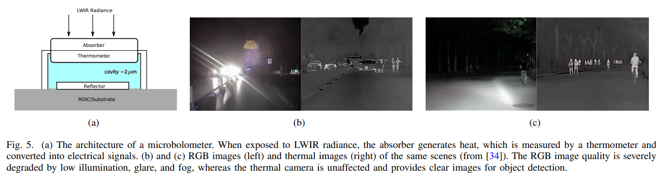
An article titled "Trilobite-inspired neural nanophotonic light-field camera with extreme depth-of-field" by Q. Fan et al. proposes a metalens design inspired by the bi-focal vision system of an extinct marine arthropod.

Abstract
A unique bifocal compound eye visual system found in the now extinct trilobite, Dalmanitina socialis, may enable them to be sensitive to the light-field information and simultaneously perceive both close and distant objects in the environment. Here, inspired by the optical structure of their eyes, we demonstrate a nanophotonic light-field camera incorporating a spin-multiplexed bifocal metalens array capable of capturing high-resolution light-field images over a record depth-of-field ranging from centimeter to kilometer scale, simultaneously enabling macro and telephoto modes in a snapshot imaging. By leveraging a multi-scale convolutional neural network-based reconstruction algorithm, optical aberrations induced by the metalens are eliminated, thereby significantly relaxing the design and performance limitations on metasurface optics. The elegant integration of nanophotonic technology with computational photography achieved here is expected to aid development of future high-performance imaging systems.

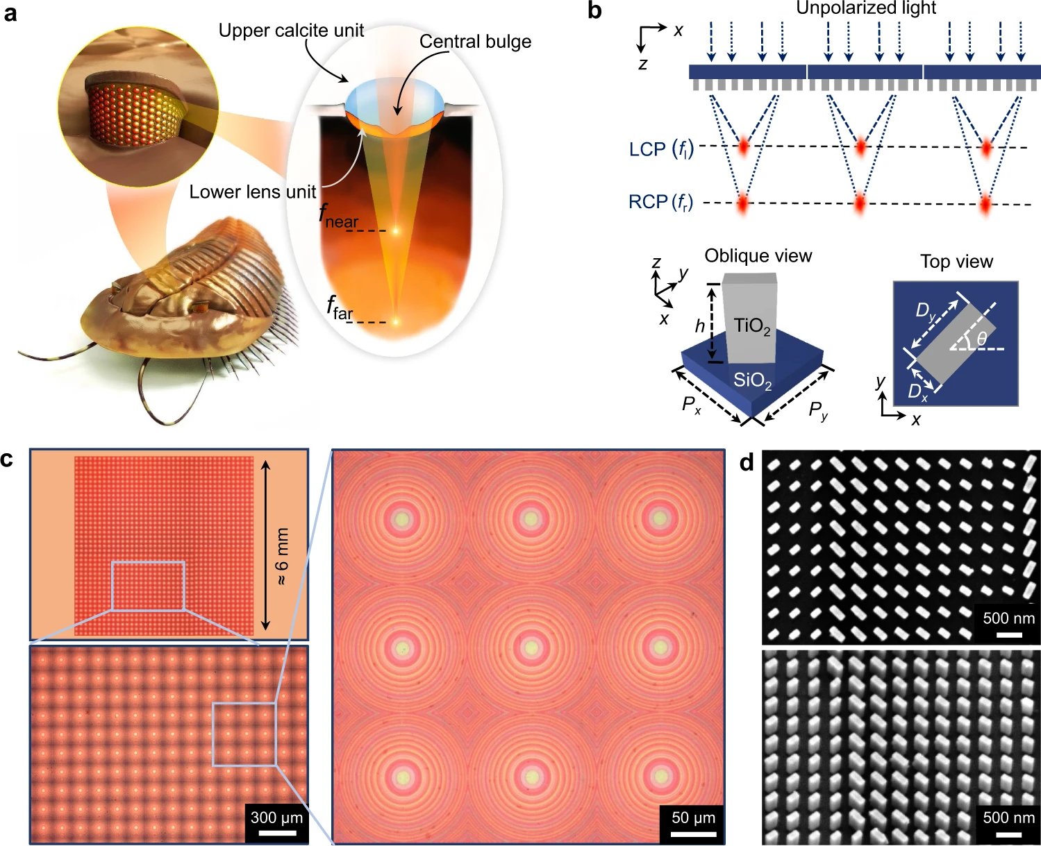
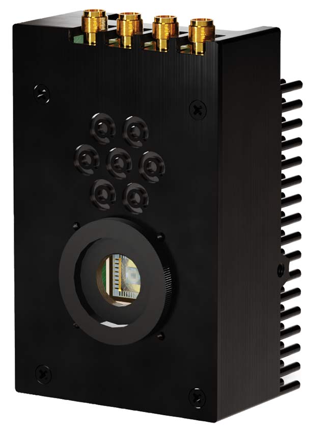
a Conceptual sketch of extinct trilobite Dalmanitina socialis and its compound eyes. Each compound eye, composed of a lower lens unit and an upper lens unit with central bulge, can simultaneously focus the incident light to near and far point, similar to a coaxial bifocal lens. b The bioinspired photonic spin-multiplexed metalens array. The unit cell of metalens array is composed of rectangle amorphous TiO2 nanopillar sitting on a SiO2 substrate with Px=Py=450 nm, and height h=600 nm. c Optical microscope image of the fabricated metalens array. The right panel shows a zoomed-in image of 3 × 3 submetalens array. d The scanning electron microscopy (SEM) images show the top view and oblique view of the TiO2 nanopillars.

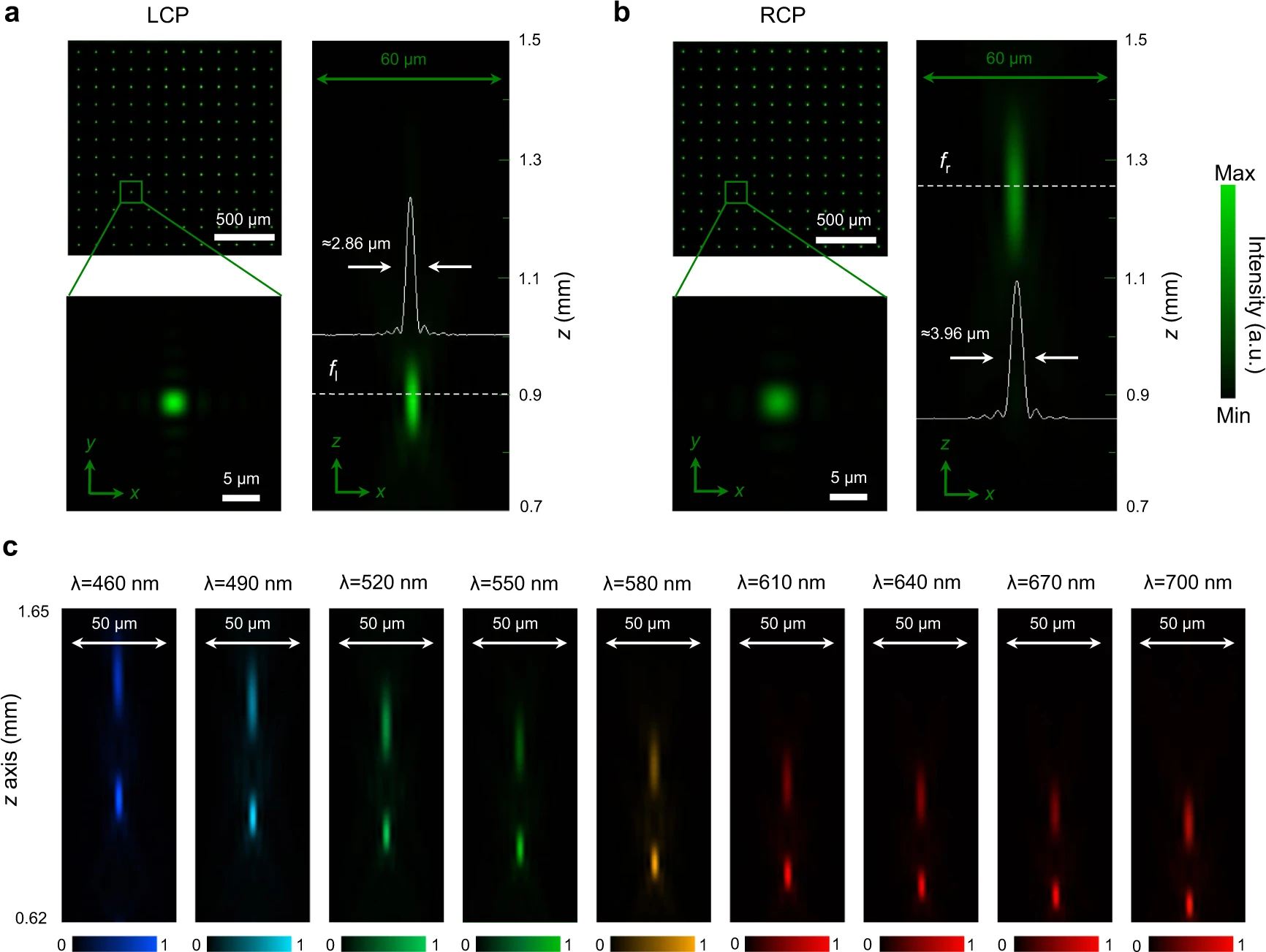
Focal spots in the x-y and x-z plane for (a) LCP and (b) RCP incident light at the wavelength of 530 nm. For ease-of-viewing, here we show an array of 12 × 12 focal spots (top left). The solid white lines show the horizontal cuts of the intensity distributions of focal spots. c Dispersion of a single submetalens illustrated by metalens focusing at different focal lengths for the wavelength spanning from 460 nm to 700 nm. The incident light is linearly polarized.

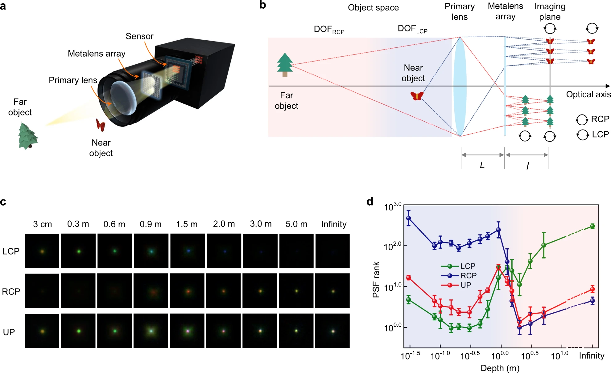
a Conceptual sketch of the proposed light-field imaging camera. b Schematic diagram of the working principle of the system with metalens array achieving spin-dependent bifocal light-field imaging. Either the LCP component of close object or the RCP component of distant object could be focused well on the identical imaging plane. The nominal distance between the primary lens and metalens array is L=47.5 mm. The nominal distance between the imaging plane and metalens array is l=0.83 mm. The focal length and aperture size of the primary lens is F=50 mm and D=6 mm, respectively. c The captured PSFs at different depths for LCP, RCP, and UP (unpolarized) incident light. d Demonstration of working range for different polarization states. The light-blue region and light-red region represent the working range of LCP and RCP components, respectively. The vertical axis represents the PSF ranks, for which the smaller value corresponds to better imaging quality. The uncertainties are standard deviation for repeated measurements (six in total).


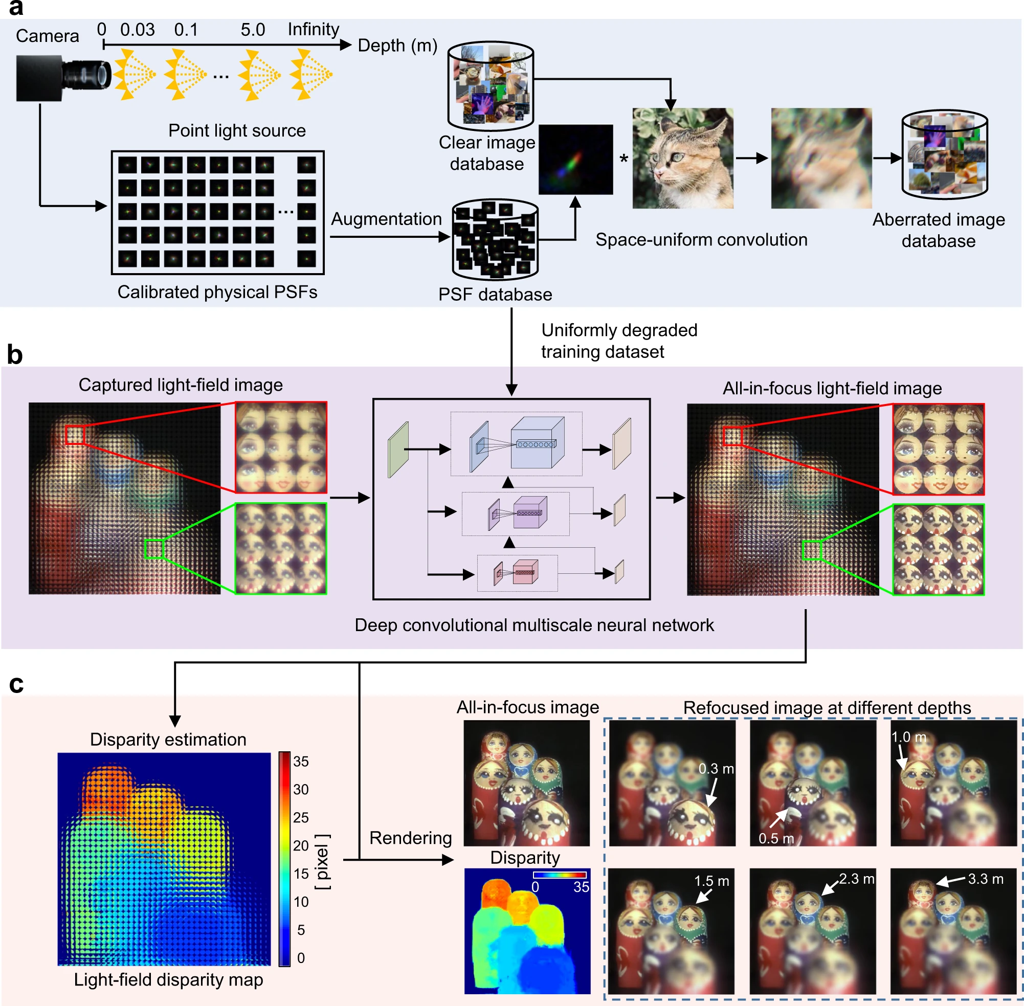
a PSF capture and training-data generation. b Aberration removal with the proposed multiscale deep convolutional neural network. The distance between the primary lens and Matryoshka nesting dolls: 0.3 m, 0.5 m, 1.0 m, 1.5 m, 2.3 m, and 3.3 m. The insets show the nearest and farthest Matryoshka nesting dolls. c Light-field processing based on the retrieved all-in-focus light-field images, including disparity estimation and refocusing images at different depths. 


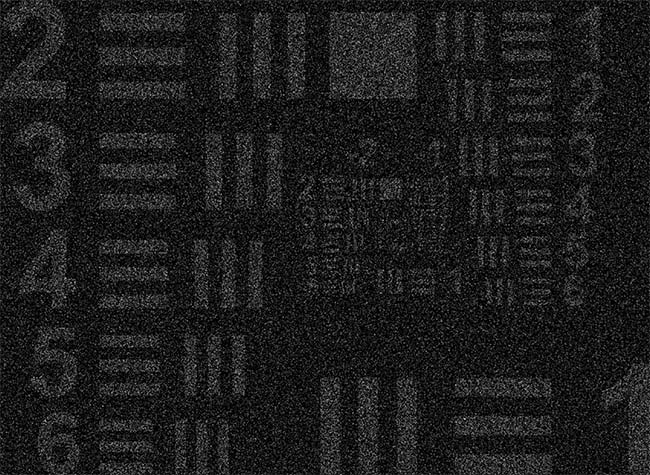
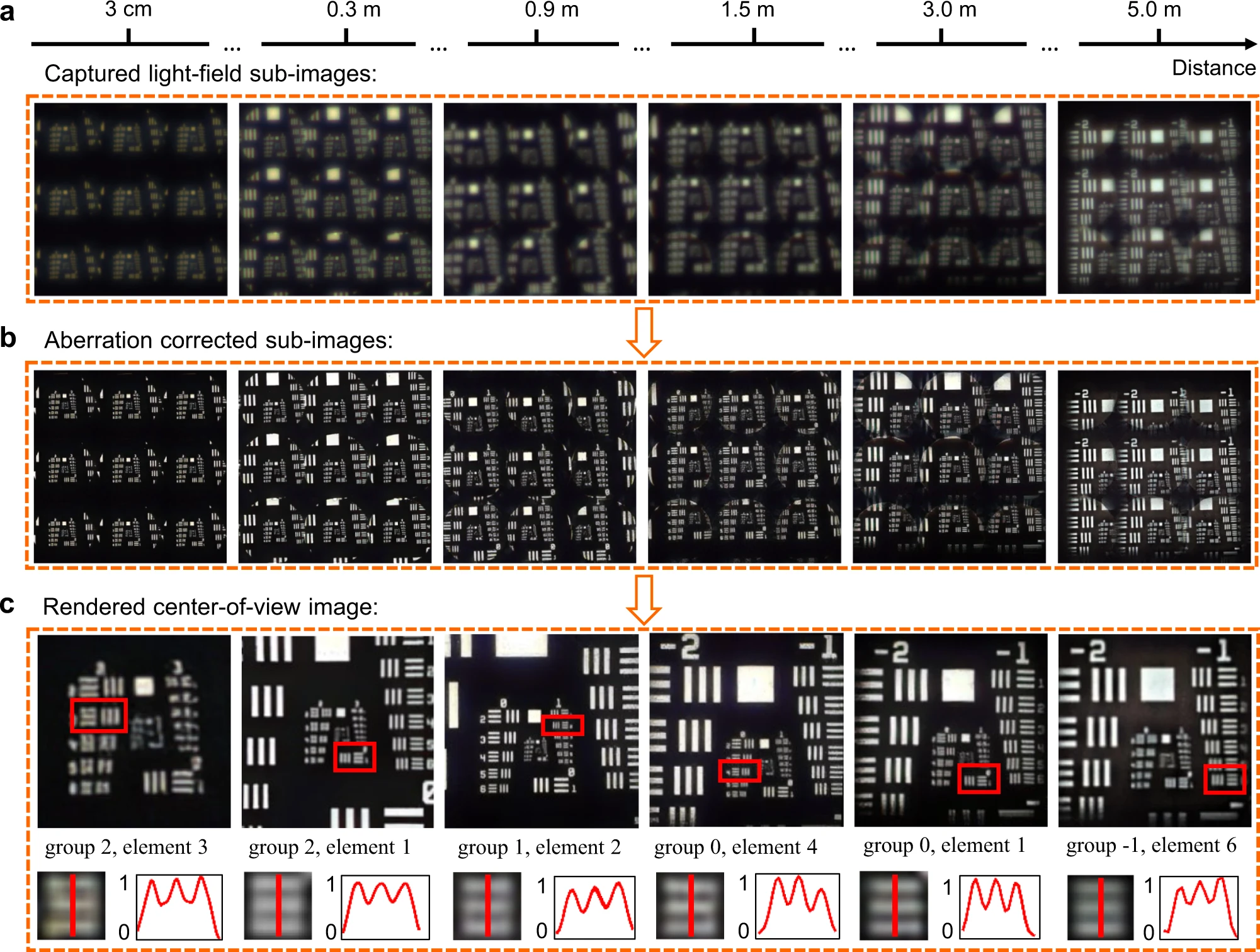
a Captured subimages of a USAF 1951 resolution chart at different depths. For easy recognition, here we show the 3×3 subimages. b Aberration-corrected subimages. c Top: Rendered center-of-view images of the USAF 1951 resolution chart. Bottom: Zoom-in images and intensity cross sections of each smallest-resolvable line pair in the resolution chart.


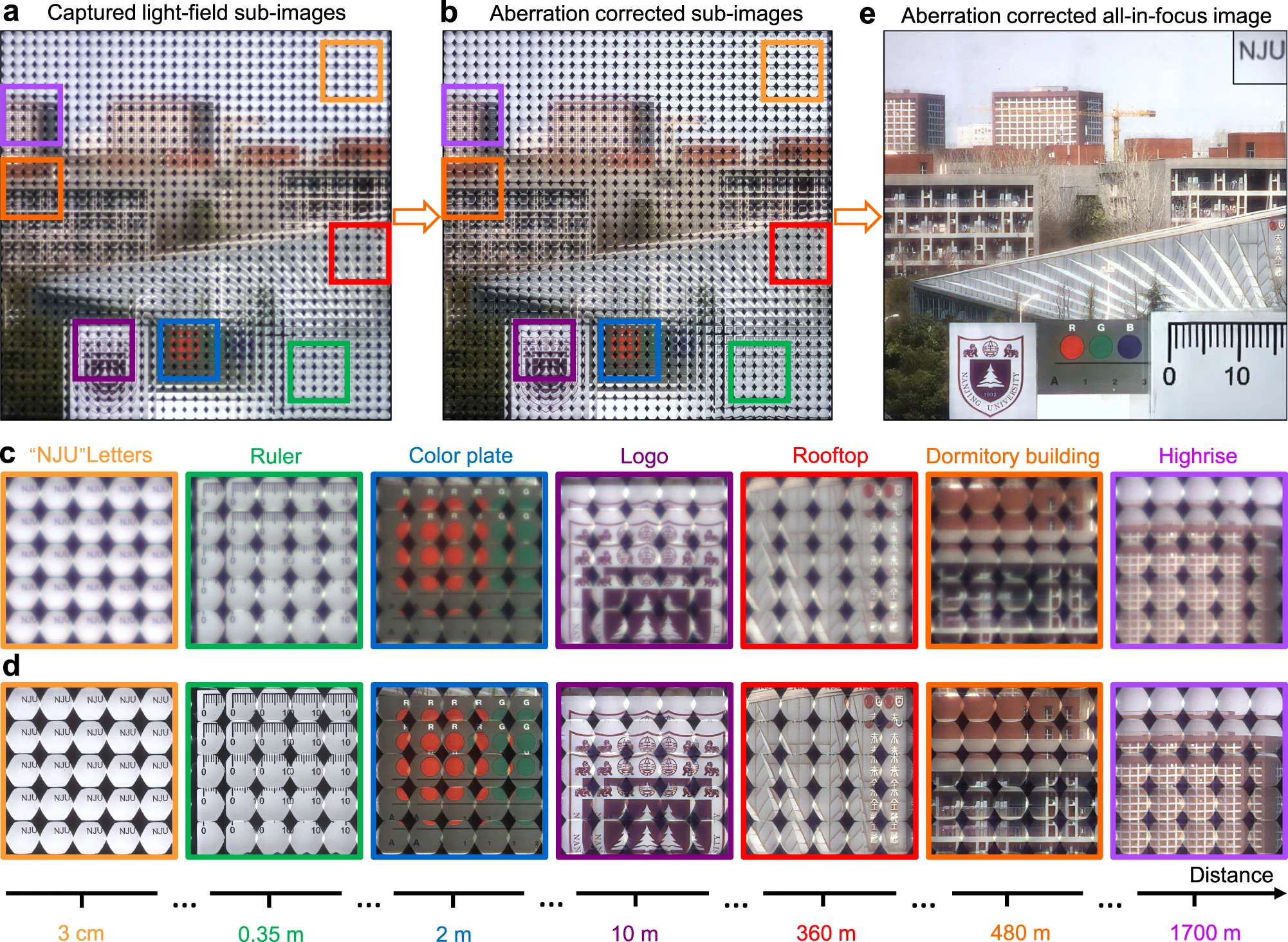
a, b Captured light-field subimages of the whole scene under natural light (a) before and (b) after aberration correction. c, d Zoomed-in subimages of different objects corresponding to the marked ones shown in (a, b), respectively. e Aberration-corrected all-in-focus image after rendering. The reconstructed NJU characters have been reasonably shifted and scaled for easy viewing.


Link: https://www.nature.com/articles/s41467-022-29568-y

Monday, May 02, 2022

"Photon counting cameras for quantum imaging applications" Prof. Edoardo Charbon

"Photon counting cameras for quantum imaging applications" 

Prof. Edoardo Charbon, Full Professor, Advanced Quantum Architecture Lab

Abstract:

Photon counting has entered the realm of image sensing with the creation of deep-submicron CMOS SPAD technology. The format of SPAD image sensors has expanded from 8×4 pixels in 2004 to the recent megapixel camera in 2019, and the applications have literally exploded in the last few years, with the introduction of proximity sensing and portable telemeters. SPAD image sensors are today in almost every smartphone and will soon be in every car. The introduction of Quanta Burst Photography has created a great opportunity for photon counting cameras, which are ideally suited for it, given its digital nature and speed; it is however computationally intensive. A solution to this problem is the use of 3D stacking, introduced for SPADs in 2015, where large silicon real estate is now available to host deep-learning processors, neural networks directly on chip, thus enabling complex processing in situ and reducing the overall power consumption. But the real opportunity is the emergence of a variety of quantum imaging modalities, including ghost imaging, quantum plenoptic vision, quantum LiDAR, to name a few. The talk will conclude with a technical and economic perspective on SPAD imagers and the vision for massively parallel solid-state photon counting in scientific and consumer applications.