Friday, December 30, 2022

News: Xenics acquired by Photonis; Omnivision to cut costs

Xenics acquired by Photonis

https://www.imveurope.com/news/xenics-bought-photonis-infrared-tech

Infrared imager maker, Xenics, has been acquired by Photonis, a manufacturer of electro-optic components.

Photonis’ components are used in the detection and amplification of ions, electrons and photons for integration into a variety of applications such as night vision optics, digital cameras, mass spectrometry, physics research, space exploration and many others. The addition of Xenics will bring high-end imaging products to Photonis’ B2B customers.

Jérôme Cerisier, CEO of Photonis, said: “We are thrilled to welcome Paul Ryckaert and the whole Xenics team in Photonis Group. With this acquisition, we are aiming to create a European integrated leader in advanced imaging in high-end markets. We will together combine our forces to strengthen our position in the infrared imaging market.”

Xenics employs 65 people across the world and its headquarters based in Leuven, Belgium.
Paul Ryckaert, CEO of Xenics, said: “By combining its strengths with the ones of Photonis Group, Xenics will benefit from Photonis expertise and international footprint which will allow us to accelerate our growth. It is a real opportunity to boost our commercial, product development and manufacturing competences and bring even more added value to our existing and future customers.” 

[Post title has been corrected as of January 8. Thanks to the commenters for pointing it out. Apologies for the error. --AI]

Wednesday, December 28, 2022

Videos of the day [TinyML and WACV]

Event-based sensing and computing for efficient edge artificial intelligence and TinyML applications
Federico CORRADI, Senior Neuromorphic Researcher, IMEC

The advent of neuro-inspired computing represents a paradigm shift for edge Artificial Intelligence (AI) and TinyML applications. Neurocomputing principles enable the development of neuromorphic systems with strict energy and cost reduction constraints for signal processing applications at the edge. In these applications, the system needs to accurately respond to the data sensed in real-time, with low power, directly in the physical world, and without resorting to cloud-based computing resources.
In this talk, I will introduce key concepts underpinning our research: on-demand computing, sparsity, time-series processing, event-based sensory fusion, and learning. I will then showcase some examples of a new sensing and computing hardware generation that employs these neuro-inspired fundamental principles for achieving efficient and accurate TinyML applications. Specifically, I will present novel computer architectures and event-based sensing systems that employ spiking neural networks with specialized analog and digital circuits. These systems use an entirely different model of computation than our standard computers. Instead of relying upon software stored in memory and fast central processing units, they exploit real-time physical interactions among neurons and synapses and communicate using binary pulses (i.e., spikes). Furthermore, unlike software models, our specialized hardware circuits consume low power and naturally perform on-demand computing only when input stimuli are present. These advancements offer a route toward TinyML systems composed of neuromorphic computing devices for real-world applications.


Monday, December 26, 2022

VoxelSensors and OQmented collaborate on laser scanning-based 3D perception to blend the physical with digital worlds

https://www.globenewswire.com/news-release/2022/12/20/2576935/0/en/VoxelSensors-and-OQmented-collaborate-on-laser-scanning-based-3D-perception-to-blend-the-physical-with-digital-worlds.html

BRUSSELS, Belgium and ITZEHOE, Germany, Dec. 20, 2022 (GLOBE NEWSWIRE) -- VoxelSensors, the inventor of Switching Pixels®, a revolutionary 3D perception technology, and OQmented, the technology leader in MEMS-based AR/VR display and 3D sensing solutions, have entered a strategic partnership. The collaboration focuses on the system integration and commercialization of a high-performance 3D perception system for AR/VR/MR and XR devices. Both companies will demonstrate this system and their technologies during CES 2023 in Las Vegas.


Switching Pixels® resolves major challenges in 3D perception for AR/VR/MR/XR devices. The solution is based on laser beam scanning (LBS) technology to deliver accurate and reliable 3D sensing without compromising on power consumption, data latency or size. VoxelSensors’ key patented technologies ensure optimal operation under any lighting condition and with concurrent systems. Their new sensor architecture provides asynchronous tracking of an active light source or pattern. Instead of acquiring frames, each pixel within the sensor array only generates an event upon detecting active light signals, with a repetition rate of up to 100 MHz.


This system is enabled through OQmented’s unique Lissajous scan pattern: in contrast to raster scanning which works line by line to complete a frame, the Lissajous trajectories scan much faster and are created very power efficiently. They can capture complete scenes and fast movements considerably quicker and require less data processing. That makes this particular technique essential for the low latency and the power efficiency of the combined perception system.


“The partnership with VoxelSensors is a great opportunity to unlock the potential of Lissajous laser beam scanning for 3D perception in lightweight Augmented Reality glasses,” said Ulrich Hofmann, co-CEO/CTO and co-founder of OQmented. “We are proud to deliver the most efficient scanning solution worldwide which enables the amazing products of our partner, bringing us one step closer to our goal of allowing product developers to build powerful but also stylish AR glasses.”


“At VoxelSensors, we wanted to revolutionize the perception industry. For too long, innovation in our space has focused on data processing, while there is so much efficiency to gain when working on the boundaries of photonics and physics. Combined with OQmented technology, we have the ability to transform the industry, enabling strong societal impact in multiple verticals, such as Augmented and Virtual Reality,” explains Johannes Peeters, founder and CEO of VoxelSensors. “Blending the physical and virtual worlds will create astonishing experiences for consumers and productivity gains in the enterprise world.”


This cooperation between two fabless deep tech semiconductor startups demonstrates Europe’s innovation capabilities in the race to produce next-generation technologies for AR/XR/VR and many other applications. These are crucial to Europe’s strategic objective of increasing its market share in semiconductors through key contributions of EU fabless companies as part of the European Chips Act.

Yole Insights article on a "meh" year for the CIS market

Original article available here: https://www.yolegroup.com/strategy-insights/cmos-image-sensor-snapshot-not-all-doom-and-gloom-good-news-is-also-stacking-up/

CMOS Image Sensor snapshot: not all doom and gloom, good news is also stacking up 

In the CMOS Image Sensor Monitor Q4 2022, Yole Intelligence, part of Yole Group, announces it expects the CMOS Image Sensors (CIS) industry to show a slight revenue decrease of -0.7% YoY in 2022, with a market value of $21.2B. This estimate takes into account the many events in 2022’s first 3 quarters; the downward revision of smartphone sales, the ongoing inventory reduction from most players in the electronics supply chains, and the continued Covid-19-related disruptions in China. 

2021 was a year of growth for CIS, reaching an all-time high of $21.3B in revenue with a relatively small annual growth of 2.8%. The key driver was the rebound in sales of smartphones, computer laptops, and tablets during the year amid the reopening of western economies after severe Covid-19-related lockdowns. Our hope for 2022 was a continuation of this improving trend. We knew the Huawei ban contributed to some inventory build-up in 2020, which had to be cleared in 2021 and maybe 2022. Our expectation for the smartphone market in 2022 was, unfortunately, too high, which translated directly into lost revenue for CIS.

In the past, the increase in the number of cameras per phone would more than compensate for smartphone volume sales declines, but not in 2022. Huawei was the actor adding the greatest number of cameras per phone, and losing such a player in the geopolitical battle has flattened the growth statistic of cameras per phone. Does it mean consumers have lost interest in high-quality phone cameras? Not at all!


Video creation using smartphones is at an all-time high due to the short-video craze. The emergence of TikTok, the favored social media of the younger generation, has been quickly copied by large incumbents, resulting in YouTube shorts and Facebook reels. This demand for high-quality video hardware was temporarily over-met during the out-of-Covid-19-lockdowns of 2021, and, therefore, the first 3 quarters of 2022 saw slightly less demand. We have seen even more dramatic but similar patterns with computer laptops and tablets in which cameras played a central role during remote work/school teleconferencing.

Another market that has explosive growth right now is Automotive CIS. The Covid-19 era signaled a turning point in consumer behavior, with demand switching to Connected Autonomous Shared and Electric (CASE) vehicles loaded with semiconductor-based features. Overall, the appetite for cameras remains high, but the dominance of the weakened smartphone market translates into the deceptive -0.7% CIS growth expected for 2022.


The smartphone market is down -10% but the sales of CIS have proven relatively resilient, while other semiconductor products, such as memory, are down -12%. The main reason is technical since we are currently experiencing a limited supply of 90nm to 40nm node wafers, the main nodes for CIS, and supporting logic wafers. The prices of these legacy nodes have increased significantly, and we observed, therefore, a continuation of high average selling prices (ASP) for CIS.

At the same time, we noted a product mix shift toward more resolution and larger optical formats; this means more silicon per die and higher ASPs. In this respect, the large smartphone OEMs have different approaches; Apple and Xiaomi favor 12Mp to 48Mp resolution with large pixels, which seems to be the ultra-premium favored approach, while Samsung, Oppo, and Vivo are increasing the resolution to 64Mp and even 108Mp with smaller pixels, which appears as the mid-end favored approach. The market is, therefore, relatively well educated and understands what a good picture means, as described in our publication with DXOMARK, “Ultra-Premium Flagship Smartphones Image Performance: End-User Perspective 2021”.


This year, both Sony and OmniVision have presented products with three-layer stacks. There are two technical reasons for this. First, the “in-pixel connection” allows removing some transistors from the upper wafer layer and moving these to the second wafer layer. This improves the volume of sensing silicon in each pixel. This technology is helpful in optimizing the signal-to-noise ratio (SNR), a critical factor in improving image quality. The second reason is that the triple stack enables high-performance sensing. New uses, such as tiny AR/VR cameras, must go beyond the current rolling-shutter (RS) approach and use either global-shutter (GS), time-of-flight (ToF), or even event-based (EB) cameras. All these require more transistors per pixel than RS approaches, so a second CIS layer is more than welcome in the drive to super compact sensing cameras. The market share of these triple-stack image sensors will grow, which will add again to the increasing silicon content per camera. This trend opens a path for sustained improvement and market growth for CIS.

The 8 leading CIS players – Sony, Samsung, OmniVision, STMicroelectronics, onsemi, SK Hynix, GalaxyCore, and SmartSens – that we have been monitoring every quarter have very different business models. Sony is a hybrid IDM, manufacturing its own 12’’ CIS wafers but outsourcing logic wafers to TSMC, UMC, and possibly also Global Foundry (unconfirmed as yet). Samsung, STMicroelectronics, and SK Hynix are IDMs with some open foundry activity. OmniVision, onsemi, GalaxyCore, and SmartSens, are fabless with varying degrees of desire for internalization; onsemi now having ownership of the East Fishkill, New York fab, and GalaxyCore investing the proceeds of its IPO into a brand new 12’’ foundry. All these players have felt pain from their supply chain structure in 2021 and 2022, either from their dependencies on others or their own limited or vulnerable capabilities. The drought and fires that happened in Samsung’s Austin, Texas, fab last year and the similar events that occurred in Taiwan’s TSMC fabs are clear reminders that no one is immune to supply-side issues in the context of climate change and geopolitical uncertainties.

The next few years will be a race to add new industrial capacities, combined with renewed technological capabilities and a high level of consumer demand. Predictions are very difficult, especially if it’s about the future! With our CIS monitor quarterly publication, we make sure to stick to reality and include some accountability in our forecast. In our view, the future is bright for CIS, but large vulnerabilities exist from the economic and geopolitical context. Let us all make this a well-informed journey with the CIS Monitor publications.

Friday, December 23, 2022

In-pixel compute: IEEE Spectrum article and Nature Materials paper

A paper by Dodda et al. from a research group in the Material Science and Engineering department at Pennsylvania State University was recently published in Nature Materials. 

Link: https://www.nature.com/articles/s41563-022-01398-9

Active pixel sensor matrix based on monolayer MoS2 phototransistor array

Abstract:

In-sensor processing, which can reduce the energy and hardware burden for many machine vision applications, is currently lacking in state-of-the-art active pixel sensor (APS) technology. Photosensitive and semiconducting two-dimensional (2D) materials can bridge this technology gap by integrating image capture (sense) and image processing (compute) capabilities in a single device. Here, we introduce a 2D APS technology based on a monolayer MoS2 phototransistor array, where each pixel uses a single programmable phototransistor, leading to a substantial reduction in footprint (900 pixels in ∼0.09 cm2) and energy consumption (100s of fJ per pixel). By exploiting gate-tunable persistent photoconductivity, we achieve a responsivity of ∼3.6 × 107 A W−1, specific detectivity of ∼5.6 × 1013 Jones, spectral uniformity, a high dynamic range of ∼80 dB and in-sensor de-noising capabilities. Further, we demonstrate near-ideal yield and uniformity in photoresponse across the 2D APS array.


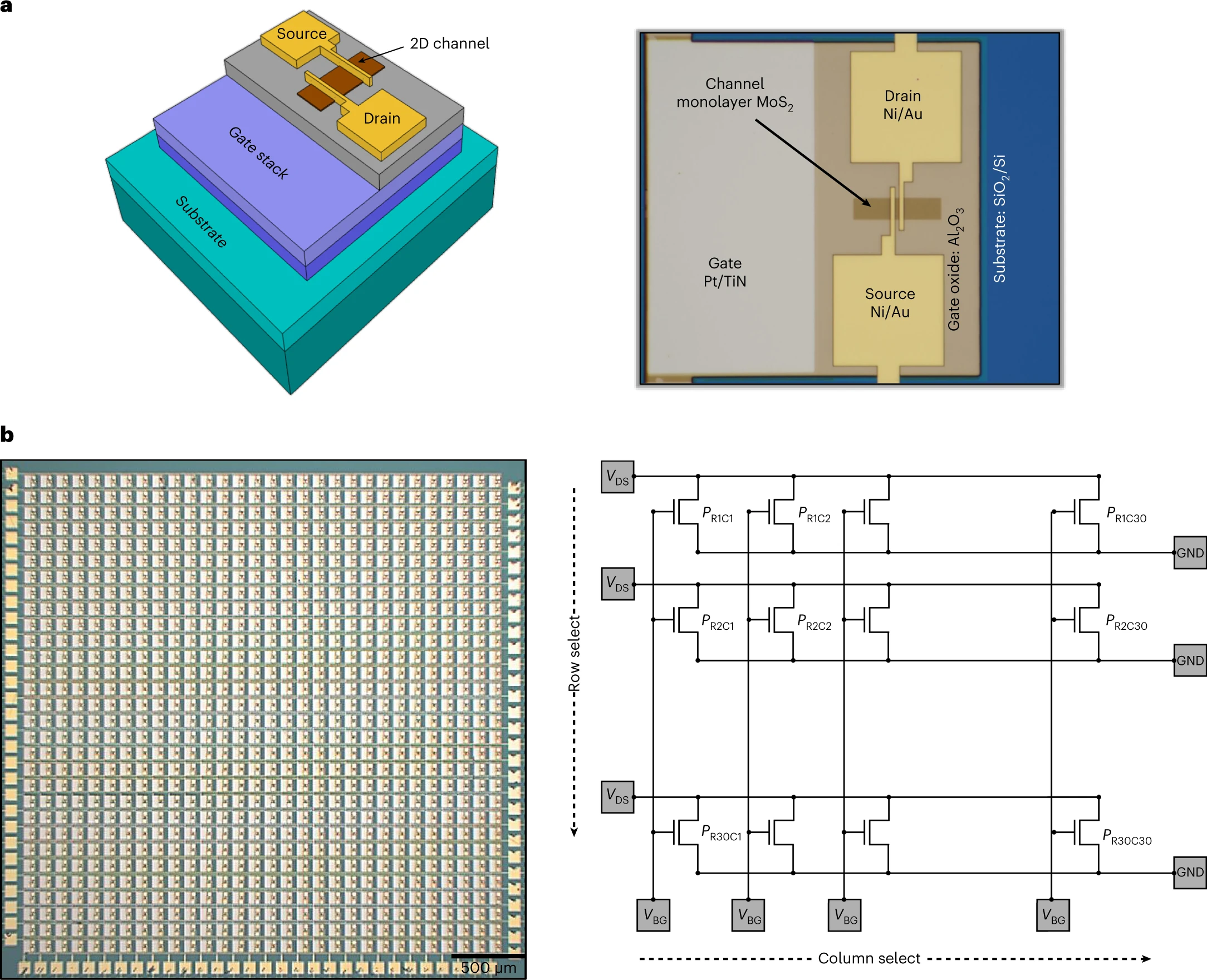
 Fig 1: 2D APS. a, 3D schematic (left) and optical image (right) of a monolayer MoS2 phototransistor integrated with a programmable gate stack. The local back-gate stacks, comprising atomic layer deposition grown 50 nm Al2O3 on sputter-deposited Pt/TiN, are patterned as islands on top of an Si/SiO2 substrate. The monolayer MoS2 used in this study was grown via an MOCVD technique using carbon-free precursors at 900 °C on an epitaxial sapphire substrate to ensure high film quality. Following the growth, the film was transferred onto the TiN/Pt/Al2O3 back-gate islands and subsequently patterned, etched and contacted to fabricate phototransistors for the multipixel APS platform. b, Optical image of a 900-pixel 2D APS sensor fabricated in a crossbar architecture (left) and the corresponding circuit diagram showing the row and column select lines (right).

Fig. 2: Characterization of monolayer MoS2. a, Structure of MoS2 viewed down its c axis with atomic-resolution HAADF-STEM imaging at an accelerating voltage of 80 kV. Inset: the atomic model of 2H-MoS2 overlayed on the STEM image. b, SAED of the monolayer MoS2, which reveals a uniform single-crystalline structure. c,d, XPS of Mo 3d (c) and S 2p (d) core levels of monolayer MoS2 film. e,f, Raman spectra (e) and corresponding spatial colourmap of peak separation between the two Raman active modes, E12g and A1g, measured over a 40 µm × 40 µm area, for as-grown MoS2 film (f). g,h, PL spectra (g) and corresponding spatial colourmap of the PL peak position (h), measured over the same area as in f. The mean peak separation was found to be ~20.2 cm−1 with a standard deviation of ~0.6 cm−1 and the mean PL peak position was found to be at ~1.91 eV with a standard deviation of ~0.002 eV. i, Map of the relative crystal orientation of the MoS2 film obtained by fitting the polarization-dependence of the SHG response shown in j, which is an example polarization pattern obtained from a single pixel of i by rotating the fundamental polarization and collecting the harmonic signal at a fixed polarization.
 
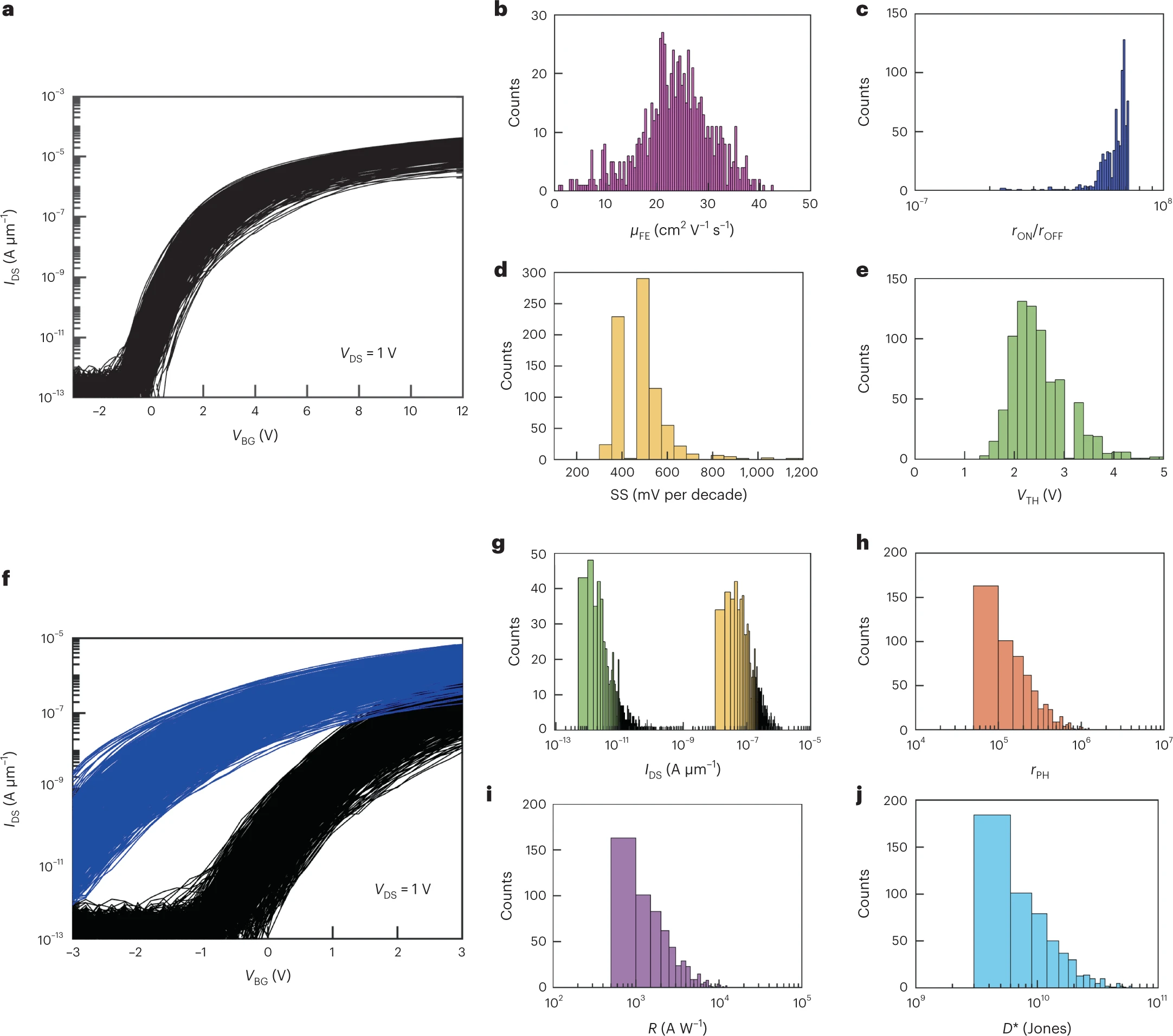
Fig. 3: Device-to-device variation in the characteristics of MoS2 phototransistors. a, Transfer characteristics, that is, source to drain current (IDS) as a function of the local back-gate voltage (VBG), at a source-to-drain voltage (VDS) of 1 V and measured in the dark for 720 monolayer MoS2 phototransistors (80% of the devices that constitute the vision array) with channel lengths (L) of 1 µm and channel widths (W) of 5 µm. b–d, Device-to-device variation is represented using histograms of electron field-effect mobility values (μFE) extracted from the peak transconductance (b), current on/off ratios (rON/OFF) (c), subthreshold slopes (SS) over three orders of magnitude change in IDS (d) and threshold voltages (VTH) extracted at an isocurrent of 500 nA µm−1 for 80% of devices in the 2D APS array (e). f, Pre- and post-illumination transfer characteristics of 720 monolayer MoS2 phototransistors after exposure to white light with Pin = 20 W m−2 at Vexp = −3 V for τexp = 1 s. g–j, Histograms of dark current (IDARK) (green) and photocurrent (IPH) (yellow) (g), the ratio of post-illumination photocurrent to dark current (rPH) (h), responsivity (R) (i) and detectivity (D*) (j), all measured at VBG = −1 V.

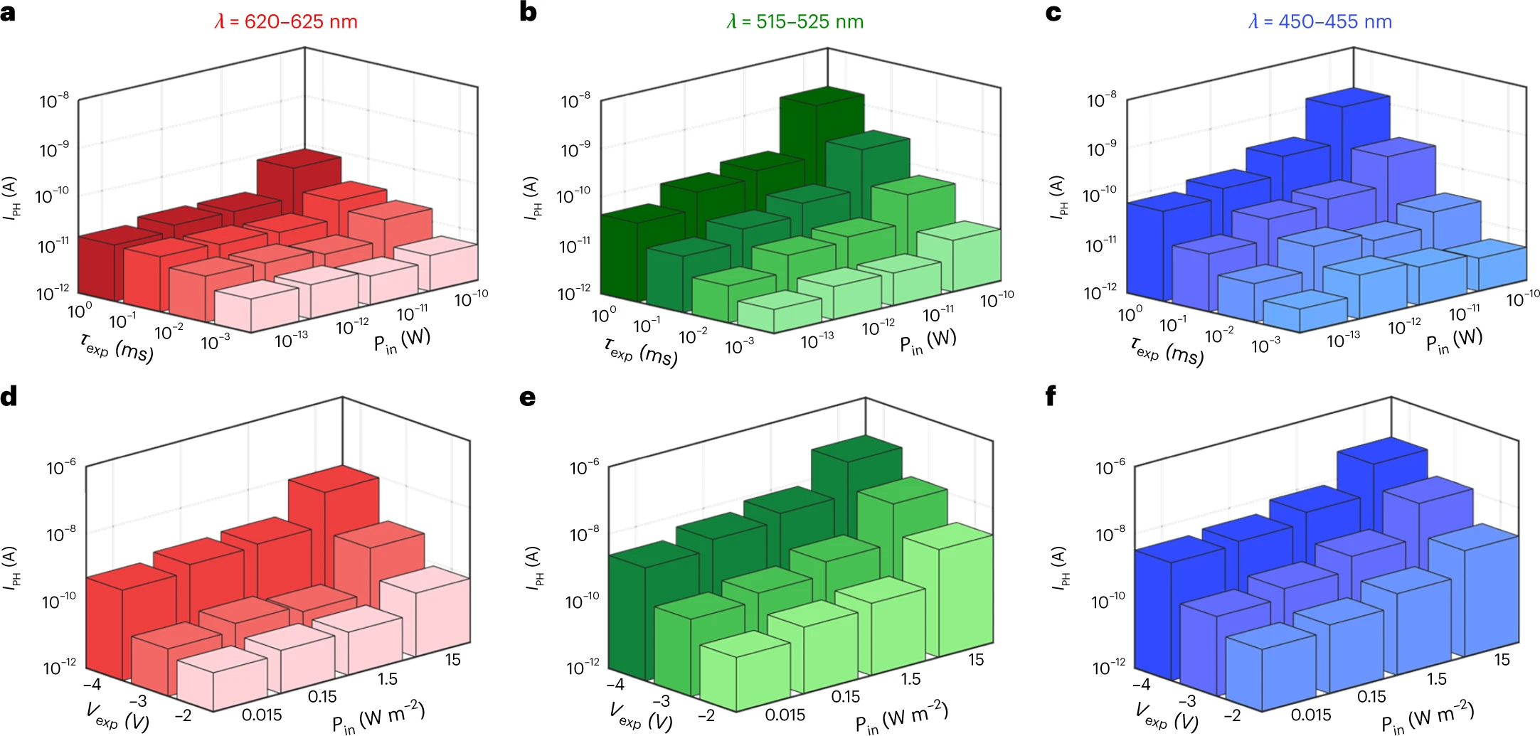
Fig. 4: HDR and spectral uniformity. a–c, The post-illumination persistent photocurrent (IPH) read out using VBG = 0 V and VDS = 1 V under different exposure times (τexp) is plotted against Pin for Vexp = −2 V at red (a), green (b) and blue (c) wavelengths. Clearly, the 2D APS demonstrates HDR for all wavelengths investigated. d–f, However, the 2D APS displays spectral non-uniformity in the photoresponse, which can be adjusted by exploiting gate-tunable persistent photoconductivity, that is, by varying Vexp. This is shown by plotting IPH against Pin for different Vexp at red (d), green (e) and blue (f) wavelengths.

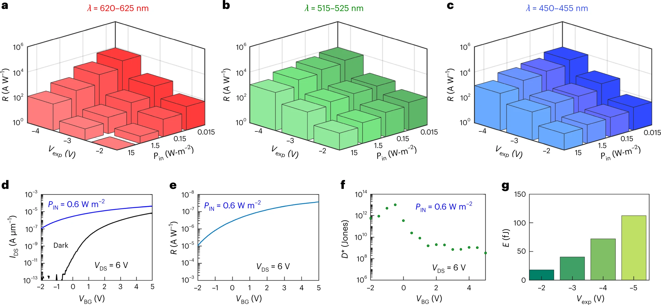
 Fig. 5: Photodetection metrics. a–c, Responsivity (R) as a function of Vexp and Pin for τexp = 100 ms for red (a), green (b) and blue (c) wavelengths. R increases monotonically with the magnitude of Vexp. d, Transfer characteristics of a representative 2D APS in the dark and post-illumination at Vexp = −6 V with Pin = 0.6 W m−2 for τexp = 200 s and VDS = 6 V. e, R as a function of VBG. For VDS = 6 V and VBG = 5 V we extract an R value of ~3.6 × 107 A W−1. f, Specific detectivity (D*) as a function of VBG at different VDS. At lower VBG, both R and Inoise, that is, the dark current obtained from d, are low, leading to lower D*, whereas at higher VBG both R and Inoise are high, also leading to lower D*. Peak D* can reach as high as ~5.6 × 1013 Jones. g, Energy consumption per pixel (E) as a function of Vexp.

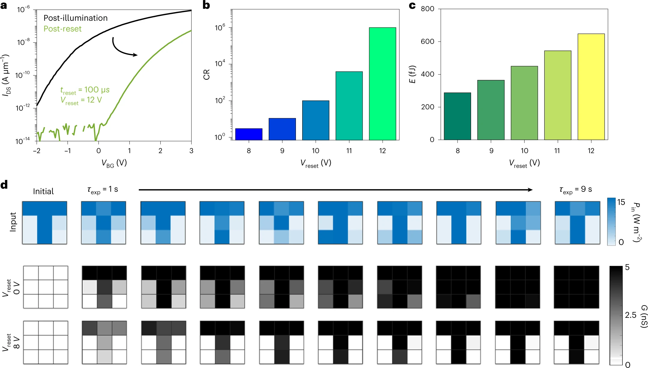
Fig. 6: Fast reset and de-noising. a, After the read out, each pixel can be reset by applying a reset voltage (Vreset) for time periods as low as treset = 100 µs. b, The conductance ratio (CR), defined as the ratio between the conductance values before and after the application of a reset voltage, is plotted against different Vreset. c, Energy expenditure for reset operations under different Vreset. d, Heatmaps of conductance (G) measured at VBG = 0 V from the image sensor with and without Vreset when exposed to images under noisy conditions. Clearly, application of Vreset helps in de-noising image acquisition.
 

This work was covered in the IEEE Spectrum magazine in an article titled "New Pixel Sensors Bring Their Own Compute: Atomically thin devices that combine sensing and computation also save power".

Link: https://spectrum.ieee.org/active-pixel-sensor

In the new study, the researchers sought to add in-sensor processing to active pixel sensors to reduce their energy and size. They experimented with the 2D material molybdenum disulfide, which is made of a sheet of molybdenum atoms sandwiched between two layers of sulfur atoms. Using this light-sensitive semiconducting material, they aimed to combine image-capturing sensors and image-processing components in a single device.

The scientists developed a 2D active pixel sensor array in which each pixel possessed a single programmable phototransistor. These light sensors can each perform their own charge-to-voltage conversion without needing any extra transistors.

The prototype array contained 900 pixels in 9 square millimeters, with each pixel about 100 micrometers large. In comparison, state-of-the-art CMOS sensors from Omnivision and Samsung have reached about 0.56 µm in size. However, commercial CMOS sensors also require additional circuitry to detect low light levels, increasing their overall area, which the new array does not... .


Special Issue of Selected Topics in Quantum Electronics: Call for Papers

Full call for papers available here: https://www.photonicssociety.org/images/files/publications/JSTQE_Single-Photon_Technologies_and_Applications_.pdf

A special issue of the IEEE Journal of Selected Topics in Quantum Electronics is soliciting articles on the topic of

Single-Photon Technologies and Applications Single-Photon Technologies and Applications


The IEEE Journal of Selected Topics in Quantum Electronics (JSTQE) invites manuscript submissions in Single-Photon Technologies and Applications. Single-photon technologies are vital to a broad range of applications such as quantum communications, optical quantum computing, quantum metrology, single-photon imaging, remote sensing and non-line-of-sight imaging. Fields such as nuclear physics, astrophysics, biology and computer vision also benefit from developments in single-photon technologies. This special issue is intended to bring together a broad range of research article with interests in single-photon sources, single-photon detectors, photon entanglement, computational imaging algorithms, and their general applications in quantum information science, 2D and 3D imaging, biomedical imaging, sensing and metrology. This special issue will address the current progress and latest breakthroughs in single-photon technologies and their emergent applications, covering among the following areas of interest:

  • Single-Photon Detectors
  • Single-Photon Sources
  • Photon-entanglement sources
  • Photon-entanglement sources
  • Integrated quantum photonics
  • Quantum communication
  • Optical quantum computing
  • Quantum metrology
  • Single-photon LIDAR
  • Novel imaging algorithms
  • Novel imaging techniques 


Primary Guest Editor: Feihu Xu, University of Science and Technology of China, China

Guest Editors:
Gerald Buller, Heriot-Watt University, UK
Martin Laurenzis, French-German Research Institute of Saint-Louis, France
Li Qian, University of Toronto, Canada
Alberto Tosi, Politecnico di Milano, Italy
Andreas Velten, University of Wisconsin at Madison, USA
Jianwei Wang, Peking University, China

Website submissions: ScholarOne Manuscripts: http://mc.manuscriptcentral.com/jstqe-pho

Submission questions: Alexandra Johnson, IEEE Journal of Selected Topics in Quantum Electronics (johnson.a@ieee.org)

Unedited preprints of accepted manuscripts are normally posted online on IEEE Xplore within one week of the final files being uploaded by the author(s) on ScholarOne Manuscripts. Posted preprints have digital object identifiers (DOIs) assigned to them and are fully citable. Once available, the preprints are replaced by final copy-edited and XML-tagged versions of manuscripts on IEEE Xplore. This usually occurs well before the hardcopy publication date. These final versions have article numbers assigned to them to accelerate the online publication; the same article numbers are used for the print versions of JSTQE. The following documents are required: PDF or MS Word manuscript (double column format, up to 12 pages for an invited paper, up to 8 pages for a contributed paper). Manuscripts over the standard page limit will have an overlength charge of $220.00 per page imposed. Biographies of all authors are mandatory, photographs are optional. See the Tools for Authors link: www.ieee.org/web/publications/authors/transjnl/index.html