A paper by Dodda et al. from a research group in the Material Science and Engineering department at Pennsylvania State University was recently published in Nature Materials.
Link: https://www.nature.com/articles/s41563-022-01398-9
Active pixel sensor matrix based on monolayer MoS2 phototransistor array
Abstract:
In-sensor processing, which can reduce the energy and hardware burden for many machine vision applications, is currently lacking in state-of-the-art active pixel sensor (APS) technology. Photosensitive and semiconducting two-dimensional (2D) materials can bridge this technology gap by integrating image capture (sense) and image processing (compute) capabilities in a single device. Here, we introduce a 2D APS technology based on a monolayer MoS2 phototransistor array, where each pixel uses a single programmable phototransistor, leading to a substantial reduction in footprint (900 pixels in ∼0.09 cm2) and energy consumption (100s of fJ per pixel). By exploiting gate-tunable persistent photoconductivity, we achieve a responsivity of ∼3.6 × 10⁷ A W−1, specific detectivity of ∼5.6 × 10¹³ Jones, spectral uniformity, a high dynamic range of ∼80 dB and in-sensor de-noising capabilities. Further, we demonstrate near-ideal yield and uniformity in photoresponse across the 2D APS array.
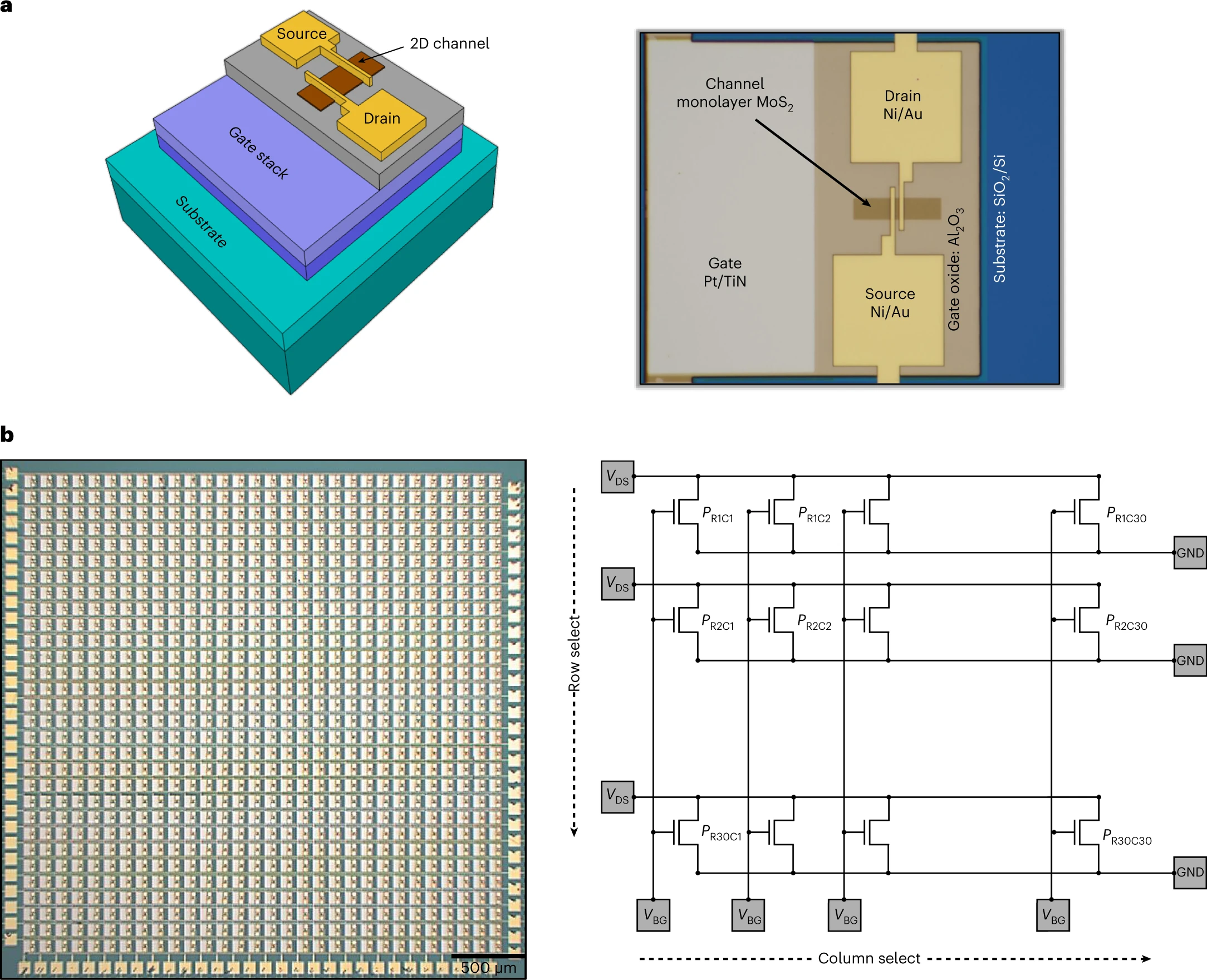
Fig 1: 2D APS. a, 3D schematic (left) and optical image (right) of a monolayer MoS2 phototransistor integrated with a programmable gate stack. The local back-gate stacks, comprising atomic layer deposition grown 50 nm Al2O3 on sputter-deposited Pt/TiN, are patterned as islands on top of an Si/SiO2 substrate. The monolayer MoS2 used in this study was grown via an MOCVD technique using carbon-free precursors at 900 °C on an epitaxial sapphire substrate to ensure high film quality. Following the growth, the film was transferred onto the TiN/Pt/Al2O3 back-gate islands and subsequently patterned, etched and contacted to fabricate phototransistors for the multipixel APS platform. b, Optical image of a 900-pixel 2D APS sensor fabricated in a crossbar architecture (left) and the corresponding circuit diagram showing the row and column select lines (right).

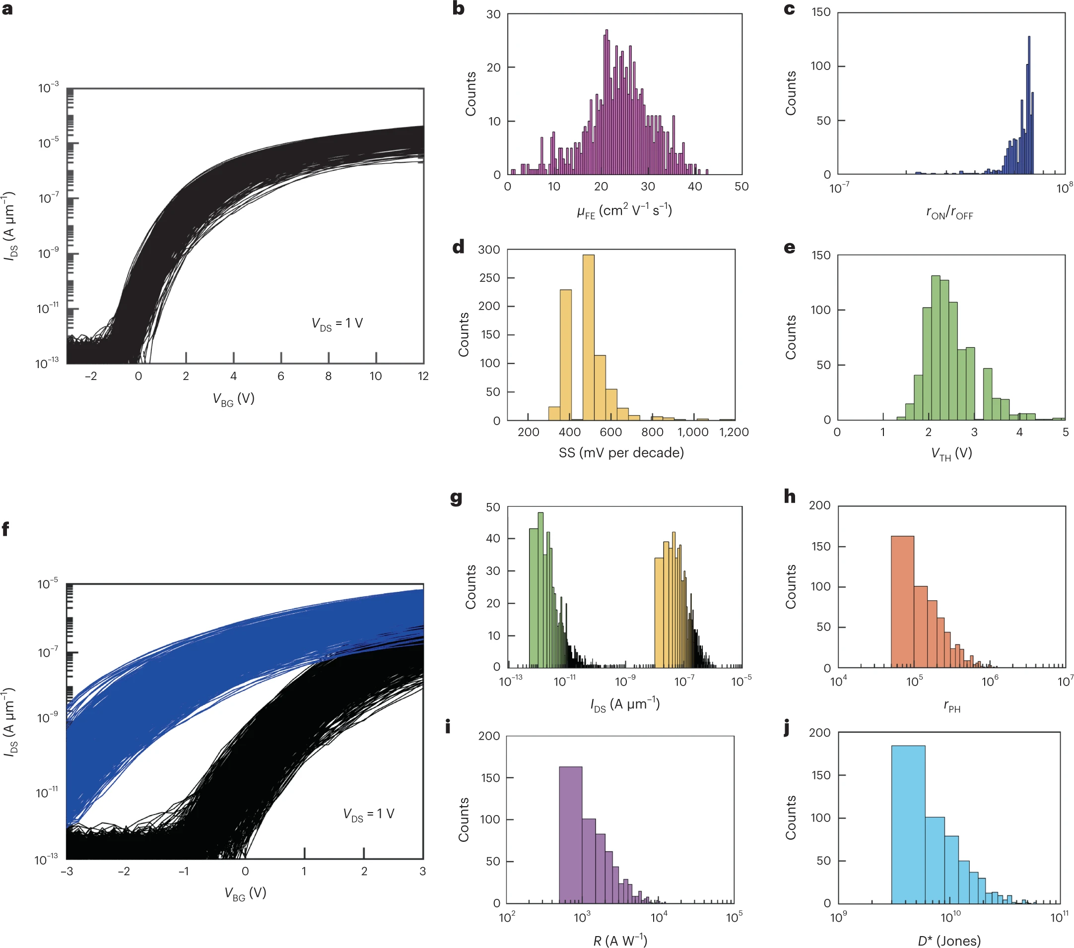
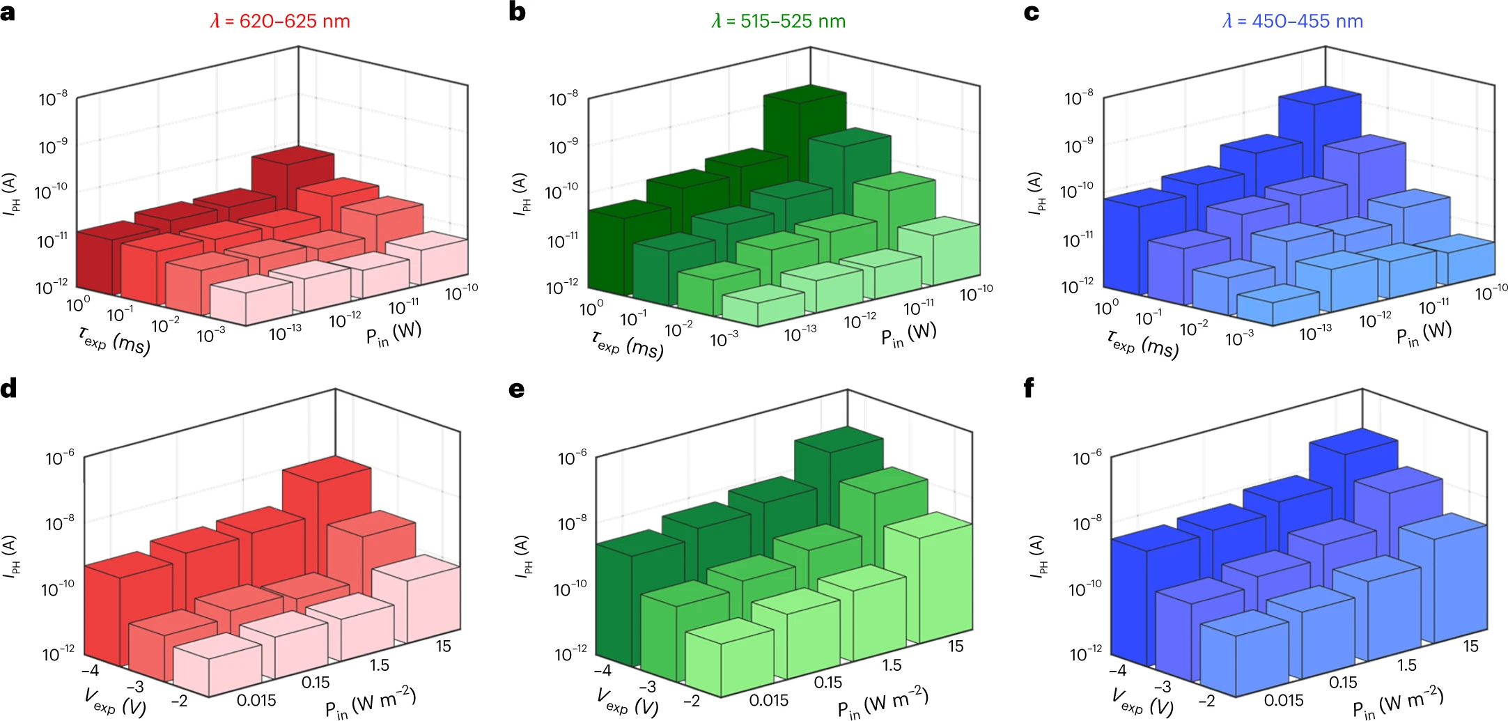
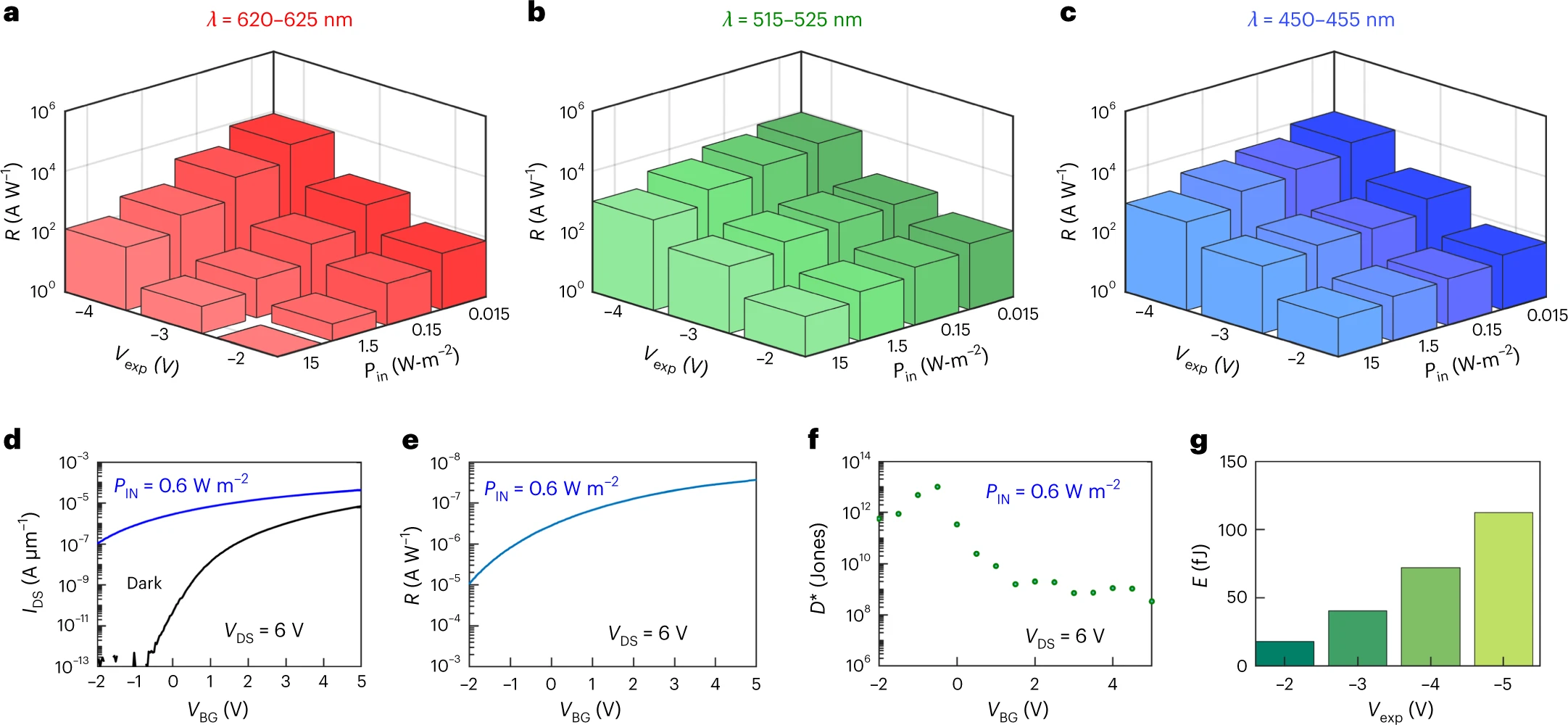
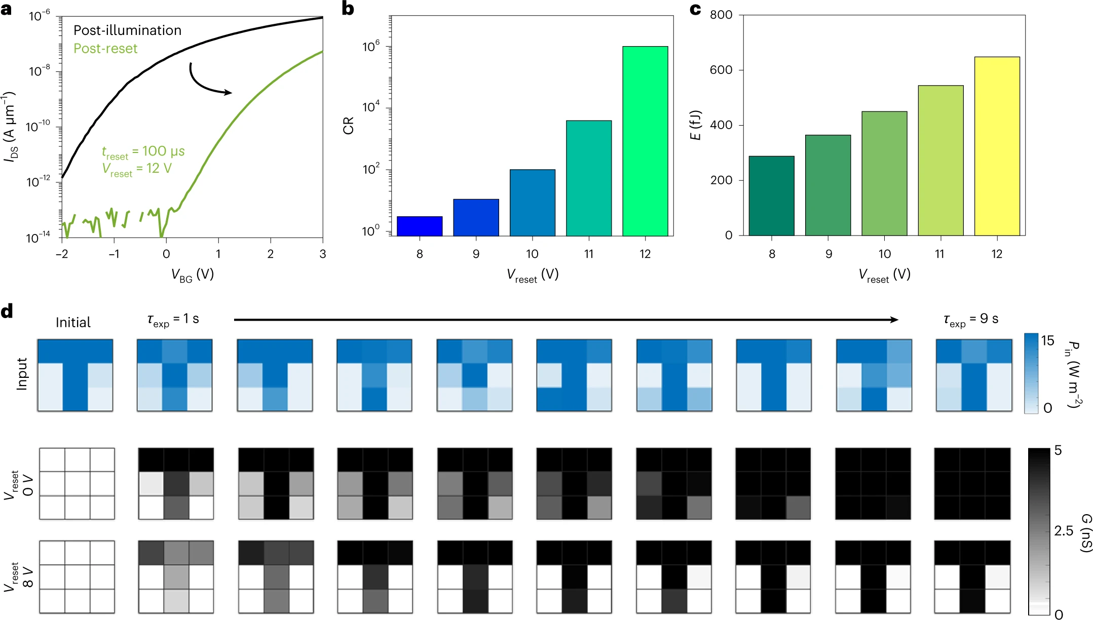
Fig. 4: HDR and spectral uniformity. a–c, The post-illumination persistent photocurrent (IPH) read out using VBG = 0 V and VDS = 1 V under different exposure times (τexp) is plotted against Pin for Vexp = −2 V at red (a), green (b) and blue (c) wavelengths. Clearly, the 2D APS demonstrates HDR for all wavelengths investigated. d–f, However, the 2D APS displays spectral non-uniformity in the photoresponse, which can be adjusted by exploiting gate-tunable persistent photoconductivity, that is, by varying Vexp. This is shown by plotting IPH against Pin for different Vexp at red (d), green (e) and blue (f) wavelengths.
This work was covered in the IEEE Spectrum magazine in an article titled "New Pixel Sensors Bring Their Own Compute: Atomically thin devices that combine sensing and computation also save power".
Link: https://spectrum.ieee.org/active-pixel-sensor
In the new study, the researchers sought to add in-sensor processing to active pixel sensors to reduce their energy and size. They experimented with the 2D material molybdenum disulfide, which is made of a sheet of molybdenum atoms sandwiched between two layers of sulfur atoms. Using this light-sensitive semiconducting material, they aimed to combine image-capturing sensors and image-processing components in a single device.
The scientists developed a 2D active pixel sensor array in which each pixel possessed a single programmable phototransistor. These light sensors can each perform their own charge-to-voltage conversion without needing any extra transistors.
The prototype array contained 900 pixels in 9 square millimeters, with each pixel about 100 micrometers large. In comparison, state-of-the-art CMOS sensors from Omnivision and Samsung have reached about 0.56 µm in size. However, commercial CMOS sensors also require additional circuitry to detect low light levels, increasing their overall area, which the new array does not... .
The conclusion that commercial sensors need large area for low noise processing is not really correct.
ReplyDelete