From: https://newsroom.st.com/media-center/press-item.html/t4598.html
Sphere Studios and STMicroelectronics reveal new details on the world’s largest cinema image sensor
Jan 11, 2024 Burbank, CA, and Geneva, Switzerland
Sensor custom created for Big Sky – the world’s most advanced camera system – and is used to capture ultra-high-resolution content for Sphere in Las Vegas
Sphere Entertainment Co. (NYSE: SPHR) today revealed new details on its work with STMicroelectronics (NYSE: STM) (“ST”), a global semiconductor leader serving customers across the spectrum of electronics applications, to create the world’s largest image sensor for Sphere’s Big Sky camera system. Big Sky is the groundbreaking, ultra-high-resolution camera system being used to capture content for Sphere, the next-generation entertainment medium in Las Vegas.
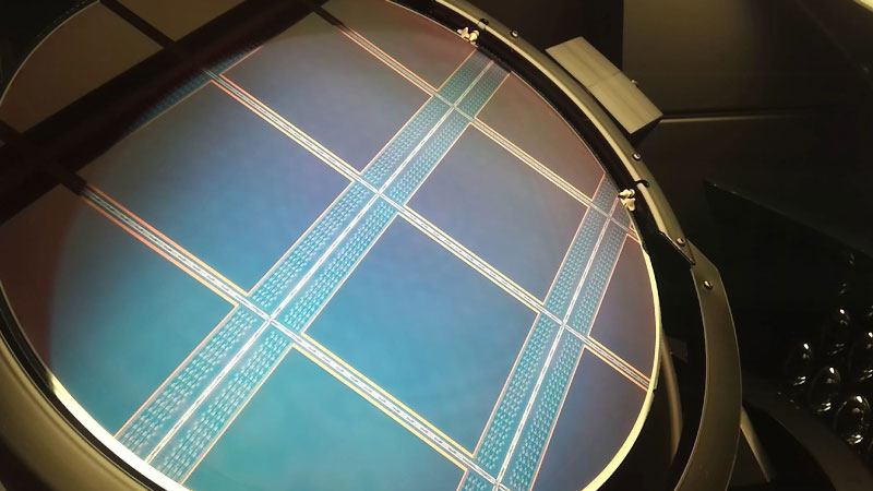
Inside the venue, Sphere features the world’s largest, high-resolution LED screen which wraps up, over, and around the audience to create a fully immersive visual environment. To capture content for this 160,000 sq. ft., 16K x 16K display, the Big Sky camera system was designed by the team at Sphere Studios – the in-house content studio developing original live entertainment experiences for Sphere. Working with Sphere Studios, ST manufactured a first-of-its-kind, 18K sensor capable of capturing images at the scale and fidelity necessary for Sphere’s display. Big Sky’s sensor – now the world’s largest cinema camera sensor in commercial use – works with the world’s sharpest cinematic lenses to capture detailed, large-format images in a way never before possible.
“Big Sky significantly advances cinematic camera technology, with each element representing a leap in design and manufacturing innovation,” said Deanan DaSilva, lead architect of Big Sky at Sphere Studios. “The sensor on any camera is critical to image quality, but given the size and resolution of Sphere’s display, Big Sky’s sensor had to go beyond any existing capability. ST, working closely with Sphere Studios, leveraged their extensive expertise to manufacture a groundbreaking sensor that not only expands the possibilities for immersive content at Sphere, but also across the entertainment industry.”
“ST has been on the cutting edge of imaging technology, IP, and tools to create unique solutions with advanced features and performance for almost 25 years,” said Alexandre Balmefrezol, Executive Vice President and Imaging Sub-Group General Manager, STMicroelectronics. “Building a custom sensor of this size, resolution, and speed, with low noise, high dynamic range, and seemingly impossible yield requirements, presented a truly novel challenge for ST – one that we successfully met from the very first wafer out of our 12” (300mm) wafer fab in Crolles, France.”
As a leader in the development and manufacturing of image sensors, ST’s imaging technologies and foundry services cater to a wide range of markets, including professional photography and cinematography. Big Sky’s 316 megapixel sensor is almost 7x larger and 40x higher resolution than the full-frame sensors found in high-end commercial cameras. The die, which measures 9.92cm x 8.31cm (82.4 cm2), is twice as large as a wallet-sized photograph, and only four full die fit on a 300mm wafer. The system is also capable of capturing images at 120 fps and transferring data at 60 gigabytes per second.
Big Sky also allows filmmakers to capture large-format images from a single camera without having to stitch content together from multiple cameras – avoiding issues common to stitching including near distance limitations and seams between images. Ten patents and counting have been filed by Sphere Studios in association with Big Sky’s technology.
Darren Aronofsky’s Postcard from Earth, currently showing at Sphere as part of The Sphere Experience, is the first cinematic production to utilize Big Sky. Since its debut, Postcard from Earth has transported audiences, taking them on a journey spanning all seven continents, and featuring stunning visuals captured with Big Sky that make them feel like they have traveled to new worlds without leaving their seats in Las Vegas. More information about The Sphere Experience is available at thesphere.com.

I wonder what they came up with first; the large screen, the sensor, or the optics? Did display tech limit the sphere's max resolution? Were manufacturing tolerances or the laws of physics the limit for the lens' resolving power? It looks like they could theoretically fit one big sensor 4X larger on that 12" wafer, but if one of the 1.2 billion pixels didn't come out right, they'd have to scrap it.
ReplyDeleteI am quite certain there will still be lot's of wafers with zero yield (depending on acceptance criteria).
DeleteYou can always push the specs of a sensor so that the yield is going to be ZERO. It is a matter of closely working with the customer/designer to come to an optimum compromise of performance (= specs) versus cost (= yield).
Delete