In a preprint titled "Metasurface-based planar microlenses for SPAD pixels", J. Vaillant et al. of STMicroelectronics and CEA LETI write:
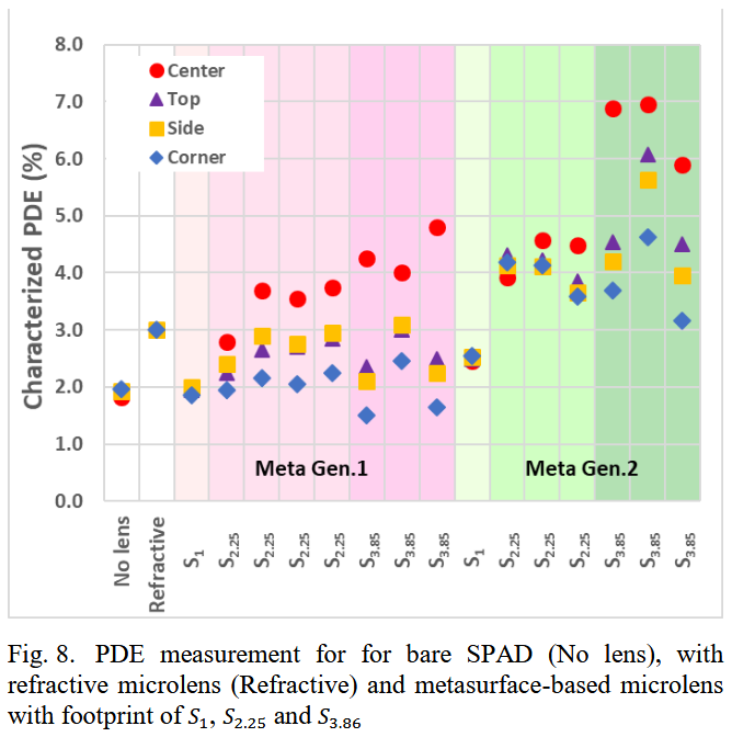
In this paper we present two design generations of metasurface-based planar microlenses implemented on Front-Side Illumination SPAD pixels. This kind of microlens is an alternative to conventional reflow microlens. It offers more degrees of freedom in term of design, especially the capability to design off-axis microlens to gather light around the SPAD photodiode. The two generations of microlenses have been fabricated on STMicroelectronics SPAD and characterized. We validated the sensitivity improvement offered by extended metasurface-based microlens. We also confirmed the impact of lithography capability on metasurface performances, highlighting the need have access to advance deep-UV lithography.


Does anyone know how to inspect the quality of these Meta-Surface (a-Si) during mass production? What would be the challenges?
ReplyDelete