Friday, January 31, 2025

SiOnyx vs Apple iPhone15 lawsuit

Link: https://appleinsider.com/articles/25/01/09/apple-fights-patent-lawsuit-over-iphone-15-camera-tech

In September, Apple was the target of a patent infringement lawsuit from SiOnyx, for allegedly encroaching on patents for full-color night vision imaging sensors.

At the time, it was claimed that Apple had infringed on the patents, referred to as "Pixel Isolation Elements, Devices, and Associated Methods," discussing improvements to photosensitive devices. By using silicon-based photonics, the complaint said that companies could create smaller, lower-cost, and higher-performance photonic devices for imaging purposes.

In December, SiOnyx amended the complaint to include that Apple had pre-suit knowledge of three patents, reports Law.com. Apple also connected in May 2014 to talk about technical developments.

In an August 2017 meeting over trench isolation structures and black silicon technology, as mentioned in the patents, SiOnyx also shared a presentation with Apple employees.

On January 8, Apple responded to the complaint by filing a motion to strike some of the new allegations. Working for Apple, attorney Michael D. Strapp of DLA Piper wanted for some of the case to be dismissed, because SiOnyx failed to state a claim.

Wednesday, January 29, 2025

Prophesee files for insolvency [Updated]

Source: https://sifted.eu/articles/startups-went-bust-2024
 

French deeptech Prophesee developed advanced ‘neuromorphic’ computer vision technology — meaning that it aimed to imitate the structure and function of the human brain and eye. In May 2024, it announced that its technology, which is mostly intended for smartphone cameras, was available in US tech giant AMD’s products. However, in October [2024], the company, which had raised €126m in total, filed for insolvency and entered judicial recovery. It told French publication Les Echos that its next round of fundraising had taken longer than expected.
[Update Jan 29 4:30pm Pacific Time] A statement from the company: 

Dear All,

The company has entered a judicial recovery procedure at the end of 2024 due to a delay in our fundraising process, which we are now in the final stages of completing with both existing and new investors.

Despite this, our operations continue as normal. My team and I remain fully committed to delivering best in class event-based sensors and solutions to our customers and partners.

Thank you for your continued support.

Cheers,
Luca Verre
CEO & Co-founder

Tuesday, January 28, 2025

ISP development short course at Electronic Imaging 2025

10xEngineers invites the Imaging and Vision community to attend a Short Course on Infinite-ISP, the open-source hardware image signal processor development package at Electronic Imaging 2025.

Date: February 6, 2025 PST

Start Time: 8:30 am - 12:45 pm Pacific Time

Duration: 4 hours


The participants of the course will be taken through the entire ISP development process using the open source Infinite-ISP package. The hands-on course touches topics such as:
a.    translating a custom algorithm written in floating-point into the hardware ISP pipeline
b.    Porting a new image sensor to the hardware ISP and tuning for a new sensor
c.    utilizing the ISP to process an available dataset for Vision or AI/ Deep Learning application

Program link: https://www.imaging.org/IST/iCore/Events/Function_Display.aspx?EventKey=E25&FunctionKey=E25/SC17

Registration: https://www.imaging.org/IST/Events/EI-Registration/SignIn.aspx

Monday, January 27, 2025

Conference List - March 2025

21st Annual Device Packaging Conference - 3-6 March 2025 - Phoenix, Arizona, USA - Website

Laser World of Photonics China - 11-13 March 2025 - Shanghai, China - Website

Image Sensors Europe - 18-19 March 2025 - London, UK - Website

MEMS & Sensors Technical Conference - 26-27 March 2025 - Atlanta, Georgia, USA - Website

If you know about additional local conferences, please add them as comments.

Return to Conference List index

Canon announces 410MP full-frame sensor

Press release: https://global.canon/en/news/2025/20250122.html

Canon develops CMOS sensor with 410 megapixels, the largest number of pixels ever achieved in a 35 mm full-frame sensor

TOKYO, January 22, 2025— Canon Inc. announced today that it has developed a CMOS sensor with 410 megapixels (24,592 x 16,704 pixels), which is the largest number1 of pixels ever achieved in a 35 mm full-frame sensor. This sensor is expected to be used in applications that demand extreme resolution in various markets including surveillance, medicine, and industry.

The newly developed CMOS sensor features a resolution equivalent to 24K (198 times greater than Full HD, and 12 times greater than 8K). This enables users to crop any part of the image captured by this sensor and enlarge it significantly while maintaining high resolution. While many CMOS sensors with a super-high pixel count are medium-format or larger, this extreme resolution sensor is compacted into a 35 mm full-frame format. This allows it to be used in combination with lenses for full-frame sensors, and it is expected to contribute to the miniaturization of shooting equipment. As data readout of a CMOS sensor tends to take longer as the number of pixels increases, achieving a CMOS sensor with a super-high pixel count requires advanced signal processing technology. The newly developed sensor employs a back-illuminated stacked formation in which the pixel segment and signal processing segment are interlayered and also includes a redesigned circuitry pattern. As a result, the sensor is capable of achieving a super-high readout speed of 3,280 megapixels per second, delivering video at 8 frames per second2.

This sensor3 also features a “four-pixel binning” function that virtually treats four adjoining pixels as one, thereby improving sensitivity and making it possible to capture brighter images. When this function is in use, the sensor can capture 100-megapixel video at 24 frames per second.

By leveraging the technology it has accumulated over many years as a leading imaging company, Canon has developed breakthrough products including CMOS sensors with super-high pixel count and ultra-sensitivity, and SPAD sensors, which detect faint traces of light even in dark areas. Canon will continue to advance its technology and contribute to the transformation and further development of society.

Additional information
The sensor is scheduled to be displayed at the Canon booth at SPIE Photonics West, a leading global conference for optics and photonics held in San Francisco from January 28-30, 2025.
 1 As of January 21, 2025 (According to a survey by Canon).
 2 Applies to both color and monochrome sensors
 3 Monochrome sensor only

Sunday, January 26, 2025

Singular Photonics launches SPAD imagers at SPIE Photonics West

Press release: https://singularphotonics.com/singular-photonics-emerges-from-stealth-with-portfolio-of-spad-based-image-sensors/

Startup introduces range of sensors with layers of advanced computation to extract valuable information from images.

Edinburgh, UK – January 23, 2025 – Singular Photonics emerged from stealth mode today, launching a new generation of image sensors based on single photon avalanche diodes (SPADs). A spin-out from the University of Edinburgh lab of digital imaging pioneer Professor Robert Henderson, Singular is one of the first companies to bring advanced computation to SPAD-based image sensing, enabling in-pixel and cross-pixel storage and computations at the lowest light levels to reveal previously invisible details of the material world and its photon events.

The company will showcase its products for the first time at next week’s SPIE Photonics West event in San Francisco.

SPADs use the “avalanche” effect in semiconductors to convert light directly into an electrical current, without the need for cooling or amplification. While most commercial SPAD-based image sensors have been limited to time-resolved counting of photons, Singular’s core innovation lies in complex layers of computation beneath 3D-stacked SPAD sensors, comparable to the way FPGAs and GPUs revolutionized parallel computing by conducting high-speed, localized processing.

Prof Henderson leads the University of Edinburgh’s CMOS Sensors and Systems Group. In 2005, he designed one of the first SPAD image sensors in nanometer CMOS technologies, leading to the first time-of-flight sensors in 2013, which today perform an autofocus-assist feature in more than a billion smartphones worldwide.

“There can be no doubt that SPAD sensors are the future of digital imaging, but their use to date in commercial devices hasn’t extended much beyond time-resolved counting of photons,” said Prof Henderson. “Computational cleverness can be the difference. We are building next-generation imaging sensors, where the computation is done digitally at the pixel level – exactly where the photons arrive.”
Simultaneously capturing depth and temporal dimensions to generate 4D images that provide deep, data-rich insights, Singular’s noiseless sensors enable more information to be extracted from light, supporting applications ranging from consumer and automotive electronics to the scientific and medical fields. The company’s approach transforms SPAD sensors into 3D stacked computational engines capable of performing a wide range of sophisticated tasks, such as real-time photon counting, timing, and advanced processing techniques, including in-pixel histograms, statistical analysis and autocorrelation.

Singular is launching with two sensors, both of which are available today:
 
Andarta, developed in collaboration with tech giant Meta, has a miniature form factor combined with high sensitivity, and is optimized for use in a number of medical imaging modalities. The sensor supports multiple modes of operation including in-pixel autocorrelation measurements, and represents a significant step closer to SPAD integration in the wearables space. For example, Andarta enables monitoring of the rate of cerebral blood flow, monitoring rapid fluctuations in light as it passes through tissue, at depths not currently possible with current sensors.

 Sirona, the company’s first product, is a 512 pixel SPAD-based line sensor capable of time-correlated single photon counting (TCSPC) and enabling Raman spectroscopy, fluorescence lifetime imaging microscopy (FLIM), time-of-flight, and quantum applications. With on-chip histogramming and time binning capability, the sensor has the potential to revolutionize spectroscopy applications.
Singular has already inked multiple deals for its sensors with some of the world’s leading instrumentation companies, and expects to announce more collaborations in 2025.

 “We are in a unique position where we already have commercially available products and are generating revenue in our first year of incorporation,” said Shahida Imani, CEO of Singular Photonics. “With new, even more advanced sensors coming to the market in 2025, we are well positioned to lead the SPAD-driven imaging revolution.”

Friday, January 24, 2025

Prof. Eric Fossum receives the National Medal of Technology and Innovation

Prof. Eric Fossum received the National Medal of Technology and Innovation at the White House on Jan 3, 2025, receiving the highest honor for technological achievement in the US.

The press briefing is no longer available [as of Jan 23, 2025, 12:00am Eastern Time]: https://www.whitehouse.gov/briefing-room/statements-releases/2025/01/03/president-biden-honors-nations-leading-scientists-technologists-and-innovators/

An archived version from Wayback Machine is available here: https://web.archive.org/web/20250104020214/https://www.whitehouse.gov/briefing-room/statements-releases/2025/01/03/president-biden-honors-nations-leading-scientists-technologists-and-innovators/

Thursday, January 23, 2025

Image sensor papers and talks at ISSCC 2025

ISSCC 2025 will be held February 16-20, 2025 in San Francisco. The program includes papers and talks of interest to the image sensors community. There will be 6 imager papers in the technical session as well as a special forum by invited industry experts on their views on technology trends.


ISSCC Imager session:
6.1 H. Shim et al., Samsung, "A 3-Stacked Hybrid-Shutter CMOS Image Sensor with Switchable 1.2μm-Pitch 50Mpixel Rolling Shutter and 2.4μm-Pitch 12.5Mpixel Global Shutter Modes for Mobile Applications"
6.2 S. Park et al., Ulsan National Institute of Technology, SolidVue, Sungkyunwan Univ., Sognag Univ., "An Asynchronous 160×90 Flash LiDAR Sensor with Dynamic Frame Rates of 5 to 250fps Based on Pixelwise ToF Validation via a Background-Light-Adaptive Threshold"
6.3 H-S. Choi et al., Yonsei Univ., KIST, XO Semiconductor, Myongji Univ, Samsung, " SPAD Flash LiDAR with Chopped Analog Counter for 76m Range and 120klx Background Light"
6.4 T-H. Tsai et al., META, Brillnics, Sesame AI, "A 400×400 3.24μm 117dB-Dynamic-Range 3-Layer Stacked Digital Pixel Sensor"
6.5 T. Kainuma et al., Sony, "A 25.2Mpixel 120frames/s Full-Frame Global-Shutter CMOS Image Sensor with Pixel-Parallel ADC"
6.6 Y. Zhuo et al., Peking Univ, Univ. of Chinese Academy of Sciences, Shanghai Inst. of Technical Physics Chinese Academy of Sciences, "A 320×256 6.9mW 2.2mK-NETD 120.4dB-DR LW-IRFPA with Pixel-Paralleled Light-Driven 20b Current-to-Phase ADC"

Forum "Seeing the Future: Advances in Image and Vision Sensing"
Image sensors are the eyes of modern technology, enabling both humans and machines to perceive and interpret the world. While they are well-known in smartphones and cameras, their role in transformative applications such as autonomous vehicles, IoT devices, and AR/VR is rapidly growing. Advances like deep-trench isolation, 3D integration, and pixel-level innovations have driven the development of 2-layer pixels, miniaturized global shutters, time-of-flight sensing, and event-based detection. Stacked architectures, in particular, enable intelligent onchip processing, making edge computing possible while reducing the device footprints for AR/VR, medical technology, and more. Metamaterials and computational cameras are further pushing boundaries by merging advanced optics with sophisticated algorithms, achieving higher image quality, enhanced depth perception, and entirely new imaging capabilities.

This forum provides engineers with insight into the latest breakthroughs in image sensor technology, edge computing, metaphotonics, and computational imaging— offering an inspiring platform to explore innovations that will shape the future of sensing and drive the next generation of technological advancements.

5.1 F. Domengie, Yole, "Innovative Image Sensors Technologies Expanding Applications and Market Frontiers"
5.2 S. Roh, Samsung, "Dispersion-Engineered Metasurface Integration for Overcoming Pixel Shrink Limitations in CMOS Image Sensors"
5.3 B. Fowler, OMNIVISION, "Advances in Automotive CMOS Image Sensors"
5.4 H.E. Ryu, Seoul National Univ., "Neuromorphic Imaging Sensor: How It Works and Its Applications"
5.5 D. Stoppa, Sony, "Innovation Trends in Depth Sensing and Imaging: Enabling Technologies and Core Building Blocks"
5.6 P. Van Dorpe, imec/KUL, "Photonics Enhanced Imaging for Omics and Medical Imaging"
5.7 C. Liu, META, "AI Sensors for Wearable Devices"
5.8 D. Golanski, STMicrolectronics, "From NIR to SWIR CMOS Image Sensors: Technology Challenges and state-of-the-art"
5.9 F. Heide, Princeton Univ, "Cameras As Nanophotonic Optical Computers"

Wednesday, January 15, 2025

Sony stacked CIS+iToF sensor (IEDM 2024)

Article (in German): https://www.pcgameshardware.de/Wissenschaft-Thema-237118/News/Fuer-Kameras-Sony-stapelt-Farb-Tiefensensor-keine-Verzerrungen-mehr-1462040/

English translation from Google Translate (with some light editing) below:


Depth sensors, which provide an image with spatial information, have become increasingly widespread in recent years. They can be used, for example, to create 3D scans or for targeted, subsequent blur effects - for example in smartphone cameras. In most cases, so-called ToF sensors (Time of Flight) are used, in which each pixel is measured when previously radiated infrared light is reflected back.

Not next to each other, but on top of each
So far, however, there has been a problem in the implementation in combination with normal camera sensors. Either the ToF sensor is located next to the camera sensor. Then there are are concealed areas through the different angles, but above all on edges, and not every color value can be assigned a depth value. Or ToF and color pixels sit on the same sensor and take away the space from each other. In other words: The resolution is reduced.

However, the camera division of Sony now claims to have found a way out. At the IEDM 2024 semiconductor trade fair, a combination sensor was presented in which the camera sensor is located directly above the depth sensor. This is made possible by the use of a new material: normally the color pixels would be located on silicon, but the broadband light would be absorbed and thus the depth pixels covered. However, Sony has apparently solved this problem by means of a new construction on a broadband transparent, organic photo-leading film. Visible wavelength hits the color sensors, while infrared light falls further down on the IR pixels of the ToF sensor.


Above each ToF pixel, which each occupies 4um, there are four RGB pixels with 1um each. In total, there is talk of a resolution of 1004 x 756 pixels for the depth map and 4016 x 3024 pixels for the color image. At least in this respect, the prototype has apparently already reached a usable area.


However, it is still unclear whether and when corresponding sensors should go into mass production. However, if Sony can potentially eliminate existing problems, the wide availability of such a sensor would offer numerous options. For example, you could simplify the creation of high-resolution 3D scans for games and movies and also make the data collection of robots significantly more reliable.

New opening in Prof Guy Meynants research group

KU Leuven

Electronics Design Engineer for Space Exploration (post-doctoral assistant) - Geel, Belgium - Link

Monday, January 13, 2025

Global shutter quantum dot image sensor for NIR imaging

L. Baudoin et al. of  ISAE SUPAERO, University of Toulouse, Toulouse, France recently published a paper titled "Global Shutter and Charge Binning With Quantum Dots Photodiode Arrays for NIR Imaging" in the IEEE Journal of the Electron Devices Society.

Open access link: https://ieeexplore.ieee.org/document/10742005

Abstract:  New applications like depth measurements or multispectral imaging require to develop image sensors able to sense efficiently in the Near Infrared and Short-Wave Infrared where silicon is weakly sensitive. Colloidal Quantum Dots (CQD) technology is an interesting candidate to address these new applications as it allows to develop image sensors with high quantum efficiency at excitonic peak and high-resolution images. In this paper, we present an electrical model describing the electrical behavior of a designed and manufactured CQD photodiode. We use this model to explore a different architecture collecting holes instead of electrons. This architecture allows to control the charge collection inside the CQD thin film through the electric field. This property enables to implement global shutter functionality, to bin charges from several photodiodes, or to operate two physically interleaved photodiodes arrays alternatively with different types of pixel circuitries. These operating modes extend the capabilities of CQD image sensors in terms of applications.

Overview of the CQD thin film properties.


(a) Electron microscopy cross section of the characterized photodiode [16] (b) Scheme of the simulated device for electrons collection (c) CQD photodiode process flow [16].


(a) CQD photodiode absorption spectrum (b) Current vs Voltage CQD photodiode characteristic – experiment vs simulation.


(a) Scheme of the simulated device for holes collection (b) Band diagram of the photodiode varying the voltage of the bottom electrode (c) Physical phenomena explaining the photodiode current vs voltage characteristic.


Current vs Voltage characteristics vs (a) CQD thin film holes mobility (b) carriers lifetime (c) CQD thin film electron affinity (d) ETL electron affinity (e) HTL electron affinity Turn-on bias vs (f) CQD thin film holes mobility (g) carriers lifetime (h) CQD thin film electron affinity (i) HTL electron affinity.


(a) Scheme of the multi-electrodes device working principle (b) Multi-electrodes photodiode architecture for holes collection control alternating collection on pixels A (top image) and collection on pixel B (bottom image).

Electrostatic potential and band diagrams explaining the carriers’ collection control for: (a) electrons collecting photodiodes (b) holes collecting photodiodes.


Current-Voltage characteristics explaining the carriers’ collection control for: (a) electrons collecting photodiodes (b) holes collecting photodiodes.


Electric field for photodiodes with central bottom electrode biased and various bottom electrodes’ widths.

Turn-on bias vs work functions for various electrodes’ size.


Current-Voltage characteristics of the collecting and non-collecting electrodes at various illuminations.

Thursday, January 09, 2025

imec SWIR quantum dot sensor

From optics.org news: https://optics.org/news/15/12/28

imec group launches SWIR sensor with lead-free quantum dot photodiodes

Technology is a step toward “greener” IR imagers for autonomous driving, medical diagnostics.

Last week, at the 2024 IEEE International Electron Devices Meeting, in San Francisco, imec, a research and innovation hub in nanoelectronics and digital technologies, and its partners in the Belgian project Q-COMIRSE, presented the first prototype shortwave infrared image (SWIR) sensor based on indium arsenide quantum dot photodiodes.

The sensor demonstrated successful 1390 nm imaging results, offering an environmentally-friendly alternative to first-generation quantum dots that contain lead, which limited their widespread manufacturing. The proof-of-concept is a critical step toward mass-market infrared imaging with low-cost and non-toxic photodiodes.

By detecting wavelengths beyond the visible spectrum, SWIR sensors can provide enhanced contrast and detail, as materials reflect differently in this range.

Face recognition and eye-tracking

These sensors can distinguish objects that appear identical to the human eye and penetrate through fog or mist, suiting them to applications such as face recognition or eye-tracking in consumer electronics, and autonomous vehicle navigation. While current versions are costly and limited to high-end applications, wafer-level integration promises broader accessibility.

Tuned for SWIR, quantum dots offer compact, low-cost absorbers, since integration into CMOS circuits and existing manufacturing processes is possible. However, first-generation QDs often contain toxic heavy metals such as lead and mercury, and the search for alternatives continues.

At 2024 IEDM, imec and its partners within the Q-COMIRSE project (Ghent University, QustomDot BV, ChemStream BV and ams OSRAM) presented a SWIR image sensor featuring a lead-free quantum dot alternative as absorber; indium arsenide (InAs). The proof-of-concept sensor, tested on both glass and silicon substrates, was the first of its kind to produce successful 1390 nm imaging results, imec announced.

Pawel Malinowski, imec technology manager and domain lead imaging, emphasized the significance of the achievement: “The first generation of QD sensors was crucial for showcasing the possibilities of this flexible platform. We are now working towards a second generation that will serve as a crucial enabler for the masses, aiming at cost-efficient manufacturing in an environmentally friendly way,” he said.

“With major industry players looking into quantum dots, we are committed to further refine this semiconductor technology towards accessible, compact, multifunctional image sensors with new functionalities.”

Stefano Guerrieri, Engineering Fellow at ams Osram, added, “Replacing lead in colloidal quantum dots with a more environmentally friendly material was our key goal in Q-COMIRSE. Our remarkable development work with imec and the others paves the way toward a low-cost and lead-free SWIR technology that, once mature for industrial products, could enable unprecedented applications in robotics, automotive, AR/VR and consumer electronics among others.”

Tuesday, January 07, 2025

Ubicept superpowers computer vision for a world in motion

Computer Vision Pioneer Ubicept to Showcase Breakthrough in Machine Perception at CES 2025


Game-Changing Photonic Computer Vision Technology Now Available for Rapid Prototyping Across Autonomous Vehicles, Robotics, AR/VR and More 


Las Vegas, January 7, 2025 – Ubicept, founded by computer vision experts from MIT, University of Wisconsin-Madison, and veterans of Google, Facebook, Skydio and Optimus Ride, today unveiled breakthrough technology that processes photon-level image data to enable unprecedented machine perception clarity and precision. The company will debut its innovation at CES 2025; demonstrations will show how the Ubicept approach handles challenging scenarios that stymie current computer vision systems, from autonomous vehicles navigating dark corners to robots operating in variable lighting conditions.

In their current state, cameras and image sensors cannot handle multiple challenging lighting conditions at the same time. Image capture in complex circumstances such as fast movement at night yields results that are too noisy or too blurry, severely limiting the potential of AI and other technologies that depend on computer vision clarity. Such systems also require different solutions to address different lighting conditions, resulting in disparate imaging systems with unreliable outputs. 

Now, Ubicept is bringing maximum visual perception to the computer vision ecosystem to make image sensors and cameras more powerful than ever before. The technology combines proprietary software with Single-Photon Avalanche Diode (SPAD) sensors -- the same technology used in iPhone LiDAR systems – to create a unified imaging solution that eliminates the need for multiple specialized cameras. This enables:

  • Crystal-clear imaging in extreme low light without motion blur

  • High-speed motion capture without light streaking

  • Simultaneous handling of bright and dark areas in the same environment

  • Precise synchronization with lights (LEDs, lasers) for 3D applications


“Ubicept has developed the optimal imaging system,” said Sebastian Bauer, cofounder and CEO, Ubicept. “By processing individual photons, we're enabling machines to see with astounding clarity across all lighting conditions simultaneously, including pitch darkness, bright sunlight, fast motion, and 3D sensing.” 

Ubicept is making its technology available via its new FLARE (Flexible Light Acquisition and Representation Engine) Development Kit, combining a 1-megapixel, full-color SPAD sensor from a key hardware partner with Ubicept’s sensor-agnostic processing technologies. This development kit will enable camera companies, sensor makers, and computer vision engineers to seamlessly integrate Ubicept technology into autonomous vehicles, robotics, AR/VR, industrial automation, and surveillance applications.

In addition to SPAD sensors, Ubicept also seamlessly integrates with existing cameras and CMOS sensors, easing the transition to next generation technologies and enabling any camera to be transformed into an advanced imaging system. 

“The next big AI wave will be enabled by computer vision powered applications in the real world; however, today’s cameras were designed for humans, and using standard image data for computer vision systems won’t get us there,” said Tristan Swedish, cofounder and CTO, Ubicept. “Ubicept’s technology bridges that gap, enabling computer vision systems to achieve ideal perception. Our mission is to create a scalable, software-defined camera system that powers the future of computer vision.”

Ubicept is backed by Ubiquity Ventures, E14 Fund, Wisconsin Alumni Research Foundation, Convergent Ventures, and other investors, with a growing customer base that includes leading brands in the automotive and AR/VR industries. 

The new FLARE Development Kit is now available for pre-order; visit www.ubicept.com/preorder to sign-up and learn more, or see Ubicept’s technology in action at CES, Las Vegas Convention Center, North Hall, booth 9467.

About Ubicept

Ubicept has pushed computer vision to the limits of physics. Developed out of MIT and the University of Wisconsin-Madison, Ubicept technology enables super perception for a world in motion by transforming photon image data into actionable information through advanced processing algorithms. By developing groundbreaking technology that optimizes imaging in low light, fast motion and high dynamic range environments, Ubicept enables industries to overcome the limitations of conventional vision systems, unlocking new possibilities for computer vision and beyond. Learn more at ubicept.com or follow Ubicept on LinkedIn

Media Contact:

Dana Zemack

Scratch Marketing + Media for Ubicept

ubicept@scratchmm.com 

Monday, January 06, 2025

Video of the day: Oculi Smart Sensing


Visual Intelligence at the Edge, by Fred Brady

Fred is currently the Chief Technical Product Officer for Oculi, a Rochester-based start-up in the smart sensing field. He presented this talk in the Society for Imaging Science and Technology (IS&T)'s Rochester NY Chapter seminar series on 11 Dec. 2024.
Today's image sensors are inefficient for vision AI - they were developed for human presence detection. These solutions are slow, power-hungry, and expensive. We will discuss Oculi's Intellipixel solution, which puts smarts at the ‘edge of the edge’ to output just the data needed for AI.
00:00 - Introduction
00:38 - Visual Intelligence at the Edge
13:00 - Oculi Output Examples
18:32 - Face and Pupil Detection
20:42 - Wrap-up
22:00 - Discussion


Friday, January 03, 2025

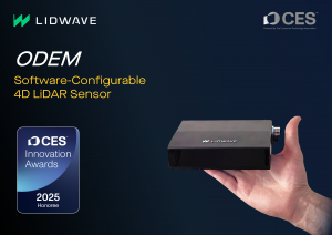
Another 2025 CES innovation award: Lidwave's 4D LiDAR sensor

From: https://www.einpresswire.com/article/768427169/lidwave-s-odem-4d-lidar-sensor-receives-the-prestigious-ces-innovation-award-2025

Lidwave's technology receives acknowledgment once more, with in the form of "CES innovation award" for its Odem 4D LiDAR sensor

JERUSALEM, ISRAEL, December 12, 2024 /EINPresswire.com/ -- Lidwave, a pioneer in the field of coherent LiDAR, is proud to share that its revolutionary Odem 4D Sensor has been recognized as an Honoree in the CES Innovation Awards 2025 in the Imaging category. Lidwave, a pioneer in the field of coherent LiDAR, is proud to share that its revolutionary Odem 4D Sensor has been recognized as an Honoree in the CES Innovation Awards 2025 in the Imaging category. “This recognition underscores Odem’s potential to redefine machine perception across industries, enabling smarter, more efficient systems, powered by Lidwave's innovative Finite Coherent Ranging (FCR™) technology” said Yehuda Vidal, Lidwave’s CEO.

At its core, Odem is a 4D coherent LiDAR that delivers both high-resolution 3D spatial data and instantaneous velocity information at the pixel level. This ability to capture an object’s location and motion in real time transforms how machines perceive and respond to their surroundings. From autonomous vehicles and robotics to industrial automation and smart infrastructure, Odem empowers systems with the precision and speed required for decision-making in dynamic environments.
One of Odem’s standout features is its software-defined architecture, which allows users to adapt key parameters - such as field of view, resolution, detection range, and frame rate – to their needs, with no change to the hardware. This flexibility enables industries to test and optimize Odem for their unique applications, making it a powerful tool for innovation across diverse sectors. Whether streamlining factory operations, enhancing transportation systems, or advancing next-generation robotics, Odem is designed to meet the evolving needs of its users.

Beyond its exceptional performance in both short- and long-range applications, Odem represents a breakthrough in scalability and affordability. By integrating a complete LiDAR system - including lasers, amplifiers, receivers, and optical routing - onto a single chip, Lidwave has made high-performance sensing technology accessible at scale. This achievement addresses one of the industry’s most critical challenges, ensuring that advanced LiDAR solutions can be deployed widely and cost-effectively.
Reliability is at the heart of Odem’s design. Built to perform under all conditions—including total darkness, glaring sunlight, fog, and dust—Odem ensures consistent and accurate detection in even the most challenging scenarios. Its robustness makes it an indispensable solution for demanding applications where precision and dependability are essential.

“We are thrilled to receive this recognition for Odem,” said Yehuda Vidal, CEO of Lidwave. “This sensor combines advanced capabilities with unmatched scalability and reliability. Its ability to provide detailed spatial and motion data in real time, while being scalable and cost-effective, is a game-changer for industries worldwide.”

“This award highlights Odem’s transformative impact,” added Dr. Yossi Kabessa, Lidwave’s CTO. “With its 4D data capabilities and flexibility, Odem empowers industries to adopt cutting-edge sensing solutions that drive innovation and progress.”

“This acknowledgment joins the feedback we get from our partners in various fields,” said Nitsan Avivi, Head of Business Development at Lidwave. “ and makes it clear that Odem will have an enormous impact on machine vision. Its unique capabilities and scalability are paving the way for new use cases, expanding the horizons of LiDAR applications”  


Wednesday, January 01, 2025

SOLiDVUE wins CES 2025 innovation award for solid-state LiDAR

From PR Newswire: https://www.prnewswire.com/news-releases/solidvue-sets-new-standards-with-ces-innovation-award-winning-high-resolution-lidar-sensor-ic-sl-2-2-302329805.html

SOLiDVUE Sets New Standards with CES Innovation Award-Winning High-Resolution LiDAR Sensor IC, 'SL-2.2'

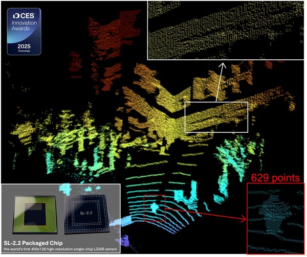
SEOUL, South Korea, Dec. 16, 2024 /PRNewswire/ -- SOLiDVUE, Korea's exclusive enterprise specialized in CMOS LiDAR (Light Detection and Ranging) sensor IC development, announced that its groundbreaking single-chip LiDAR sensor IC, the SL-2.2, boasting a world-first 400x128 resolution, has been honored with the CES Innovation Award® at CES 2025.

LiDAR is a next-generation core component for autonomous vehicles and robotics, capable of precisely measuring the shape and distance of objects to output 3D images. This technology enables accurate object recognition for applications such as autonomous vehicles, drones, robots, security cameras, and traffic management systems.

Established in 2020, SOLiDVUE focuses on designing SoCs (System-on-Chip) for LiDAR sensors, which form the core of a LiDAR system. "While mechanical LiDAR has been the standard, the latest trend is to replace it with semiconductor chips," said co-CEO, Jung-Hoon Chun. SOLiDVUE is the only company in South Korea to have developed LiDAR sensors that completely replace mechanical components with semiconductor technology.

SOLiDVUE's LiDAR sensors are compatible with solid-state LiDAR systems, which are 10 times smaller and 100 times cheaper than traditional mechanical LiDAR systems. "Our sensors offer ultra-compact chip solution compared to competitors, but their performance is not just on par—it's superior," co-CEO, Jaehyuk Choi stated confidently.

The company's proprietary technologies, such as CMOS SPAD (Single Photon Avalanche Diode) technology, single-chip sensor architecture, and image signal processor, underpin its competitive edge. CMOS SPAD technology enhances measurement accuracy by detecting sparse photons even the single-photon level. Globally, only a few companies, including SOLiDVUE, possess such single-chip sensor technology.

SOLiDVUE's technological prowess has been repeatedly acknowledged at the IEEE ISSCC (International Solid-State Circuits Conference), marking a remarkable achievement for a Korean fabless company. Furthermore, the recent CES Innovation Award has once again affirmed its prominence in the LiDAR sensor industry.

SOLiDVUE's award-winning SL-2.2 pushes the boundaries of resolution with its ability to output high-resolution 3D images up to 400x128 pixels, surpassing the 200x116 resolution of existing products. The SL-2.2 can detect objects up to 200 meters away with an exceptional 99.9% accuracy.

As a single-chip sensor, the SL-2.2 is fabricated using standard CMOS semiconductor processes and benefits from SOLiDVUE's proprietary ultra-miniaturization technology. The sensor core measures just 0.9cm x 0.9cm and is packaged in a compact 1.4cm x 1.4cm BGA-type package, enabling seamless integration into various LiDAR systems. Its single-chip design reduces power consumption, enhancing energy efficiency and ensuring high reliability.

The SL-2.2 is a successor to the company's first product, the SV-110, which features a 200x116 resolution and a 128-meter detection range. The SL-2.2 is scheduled for an official release in 2025 and is expected to play a pivotal role in advancing LiDAR technology across applications such as autonomous vehicles, robotics, drones, and smart cities.

Co-CEO Jaehyuk Choi emphasized, "At SOLiDVUE, we are actively collaborating with numerous domestic and international companies and research institutions to push the boundaries of LiDAR technology. With the rapidly growing demand for LiDAR, we are committed to continuously expanding our product lineup to meet diverse market needs. Our mission is to lead the LiDAR industry by delivering innovative solutions that address the evolving challenges of tomorrow."