Monday, December 30, 2024

MagikEye to present 5cm to 5m depth sensing solution at CES

From Businesswire: https://www.businesswire.com/news/home/20241218853081/en/MagikEye-Brings-%E2%80%9CSeeing-in-3D-from-Near-to-Far%E2%80%9D-to-CES-2025-Now-Enabling-Depth-Sensing-from-5cm-to-5m

MagikEye Brings “Seeing in 3D from Near to Far” to CES 2025: Now Enabling Depth Sensing from 5cm to 5m

STAMFORD, Conn.--(BUSINESS WIRE)--MagikEye Inc. (www.magik-eye.com), a leader in advanced 3D depth sensing technology, is pleased to offer private demonstrations of its latest Invertible Light™ Technology (ILT) advancements at the 2025 Consumer Electronics Show (CES) in Las Vegas, NV. Building on a mission to provide the “Eyes of AI,” the newest iteration of ILT can measure depth as close as 5cm and reaching to 5m. This expanded range can transform how developers take advantage of 3D vision in their products, allowing seeing 3D from near-to-far.

By leveraging a simple, low-cost projector and a standard CMOS image sensor, MagikEye’s ILT solution delivers 3D with unparalleled cost and power savings. A small amount of software running on any low-power microcontroller enables a broad spectrum of applications—ranging from consumer electronics and robotics to AR/VR, industrial automation, and transportation—without the cost of specialized silicon or sensors. With the newest version of ILT, manufacturers can inexpensively add depth capabilities to more devices, increasing product versatility and improving product performance.

“This new generation of ILT redefines what’s possible in 3D sensing,” said Takeo Miyazawa, Founder & CEO of MagikEye. “By bringing the near-field range down to 5cm, we enable a richer, more immersive interaction between devices and their environment, while providing more complete data for AI applications. From tiny consumer gadgets to large-scale robotic systems, our technology scales effortlessly, helping our customers drive innovation, enhance user experiences, and unlock new market opportunities.”

During CES 2025, MagikEye invites interested partners, product designers, and customers to arrange a private demonstration of the enhanced ILT technology. These one-on-one sessions will provide an in-depth look at how to seamlessly integrate ILT into existing hardware and software platforms and explore its potential across a multitude of applications.

Monday, December 23, 2024

Yole Webinar on Status of CIS Industry in 2024

Yole recently held a webinar on the latest trends and emerging applications in the CMOS image sensor market.

It is still available to view with a free registration at this link: https://attendee.gotowebinar.com/register/3603702579220268374?source=Yole+webinar+page

More information:

https://www.yolegroup.com/event/trade-shows-conferences/webinar-the-cmos-image-sensor-industry/


The CMOS image sensor (CIS) market, which is projected to grow at a 4.7% compound annual growth rate from 2023 to 2029, growing to $28.6 billion, is undergoing a transformation. Declining smartphone sales, along with weakening demand in devices such as laptops and tablet computers, are key challenges to growth.

We forecast that automotive cameras and other emerging applications will instead be the key drivers of future CIS market growth. Technology innovations such as triple-stacked architectures and single-photon avalanche diode-based sensors are improving performance, enabling new applications in low light and 3D imaging, for example, while high dynamic range and LED flicker mitigation are key requirements for automotive image sensors.

This webinar, co-organized with the Edge AI + Vision alliance, will discuss how CIS suppliers are focusing on enhancing sensor capabilities, along with shifting their product mixes towards higher potential value markets. Our experts will also explore how emerging sensing modalities such as neuromorphic, optical metasurfaces, short-wave infrared and multispectral imaging will supplement, and in some cases supplant, CMOS image sensors in the future.


Friday, December 20, 2024

CEA-Leti presents Integrated Phase Modulator And Sensor at IEDM 2024

CEA-Leti Device Integrates Light Sensing & Modulation, Bringing Key Scalability, Compactness and Optical-Alignment Advantages
 
First-Reported Device ‘Improves Resolution and Penetration Depth Of Optical Imaging Techniques for Biomedical Applications’
 
SAN FRANCISCO – Dec. 10, 2024 – CEA-Leti researchers have developed the first-reported device able to sense light and modulate it accordingly in a single device, using a liquid crystal cell and a CMOS image sensor.
 
The compact system provides intrinsic optical alignment and compactness and is easy to scale-up, facilitating the use of digital optical phase conjugation (DOPC) techniques in applications such as microscopy and medical imaging.
 
“The main benefits of this device, which provides significant advantages compared to competing systems that require separate components, should boost its deployment in more complex and larger optical systems,” said Arnaud Verdant, CEA-Leti research engineer in mixed-signal IC design and lead-author of the paper presented at IEDM 2024.
 
In the paper, “A 58×60 π/2-Resolved Integrated Phase Modulator And Sensor With Intra-Pixel Processing”, CEA-Leti explained that this is the first solid-state device integrating a liquid crystal-based spatial light modulator hybridized with a custom lock-in CMOS image sensor. The integrated phase modulator and sensor embeds a 58×60 pixel array, where each pixel both senses and modulates light phases.
 
The device leverages the key advantage of DOPC to dynamically compensate for optical wavefront distortions, which improves performance in a variety of photonic applications and corrects optical aberrations in imaging systems. By precisely controlling laser beams, it improves the resolution and penetration depth of optical imaging techniques for biomedical applications.
 
Standard DOPC systems rely on separated cameras and light-wavefront modulators, but their bandwidth is limited by the data processing and transfer between these devices. If the system senses and controls the light-phase modulation locally in each pixel, the bandwidth no longer depends on the number of pixels, and is only limited by the liquid crystal response time. This feature is a key advantage in fast-decorrelating, scattering media, such as living tissues.
 
“Scattering in biological tissues and other complex media severely limits the ability to focus light, which is a critical requirement for many photonic applications,” Verdant explained. “Wavefront shaping techniques can overcome these scattering effects and achieve focused light delivery. In the future, this will make it possible to envision applications such as photodynamic therapy, where light focusing selectively activates photosensitive drugs within tumors.
 
“When this technology is more mature, it also may have diverse benefits across various sectors, in addition to improving biomedical imaging resolution and depth,” he said. “It could enable earlier disease detection and non-invasive therapies. In industry, it could enhance laser beam quality and efficiency.”


Wednesday, December 18, 2024

Sub-micron InGaAs pixels

In a paper titled "Highly-efficient (>70%) and Wide-spectral (400–1700 nm) sub-micron-thick InGaAs photodiodes for future high-resolution image sensors" in Light: Science & Applications, Dae-Myeong Geum et al. from KAIST write:

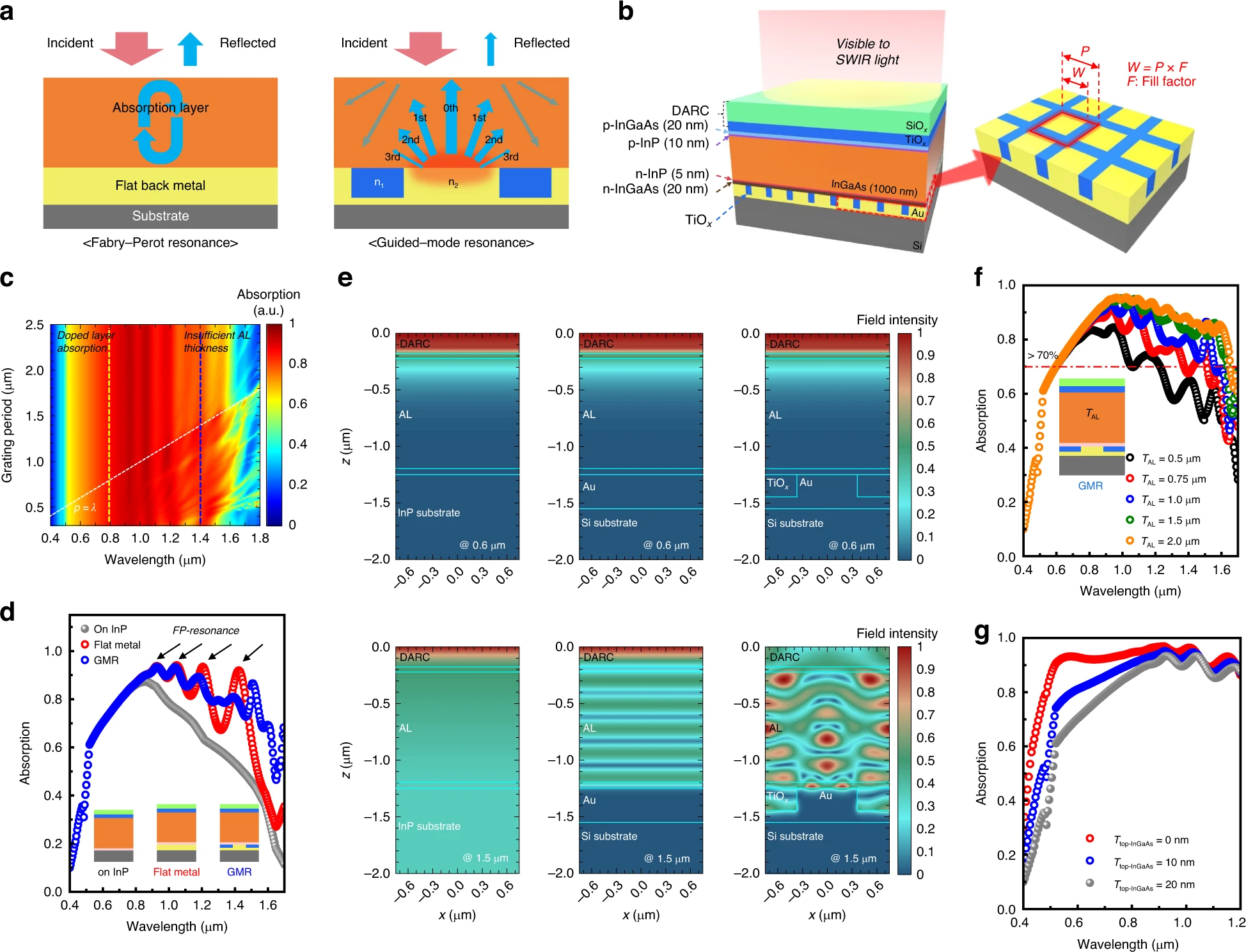
Abstract: This paper demonstrates the novel approach of sub-micron-thick InGaAs broadband photodetectors (PDs) designed for high-resolution imaging from the visible to short-wavelength infrared (SWIR) spectrum. Conventional approaches encounter challenges such as low resolution and crosstalk issues caused by a thick absorption layer (AL). Therefore, we propose a guided-mode resonance (GMR) structure to enhance the quantum efficiency (QE) of the InGaAs PDs in the SWIR region with only sub-micron-thick AL. The TiOx/Au-based GMR structure compensates for the reduced AL thickness, achieving a remarkably high QE (>70%) from 400 to 1700 nm with only a 0.98 μm AL InGaAs PD (defined as 1 μm AL PD). This represents a reduction in thickness by at least 2.5 times compared to previous results while maintaining a high QE. Furthermore, the rapid transit time is highly expected to result in decreased electrical crosstalk. The effectiveness of the GMR structure is evident in its ability to sustain QE even with a reduced AL thickness, simultaneously enhancing the transit time. This breakthrough offers a viable solution for high-resolution and low-noise broadband image sensors.

a Schematics of conventional Fabry-Perot resonance cavity and proposed GMR structure. b Design of GMR integrated InGaAs PD structures and design parameters of GMR structure. c 2D mapping results for the relative amount of absorption in AL grating period as a function of wavelength with fixed TAL = 1 μm. d RCWA simulation results with 1 μm AL PD on rear side engineering about InP substrate, flat metal structure, and GMR structure. e Electric field intensity distribution for 1.0 μm AL InGaAs PIN PDs on different bottom structures at 0.6 μm and 1.5 μm. f TAL dependent absorption spectra in terms of wavelength. g Top InGaAs layer thickness-dependent absorption spectra for visible light absorption

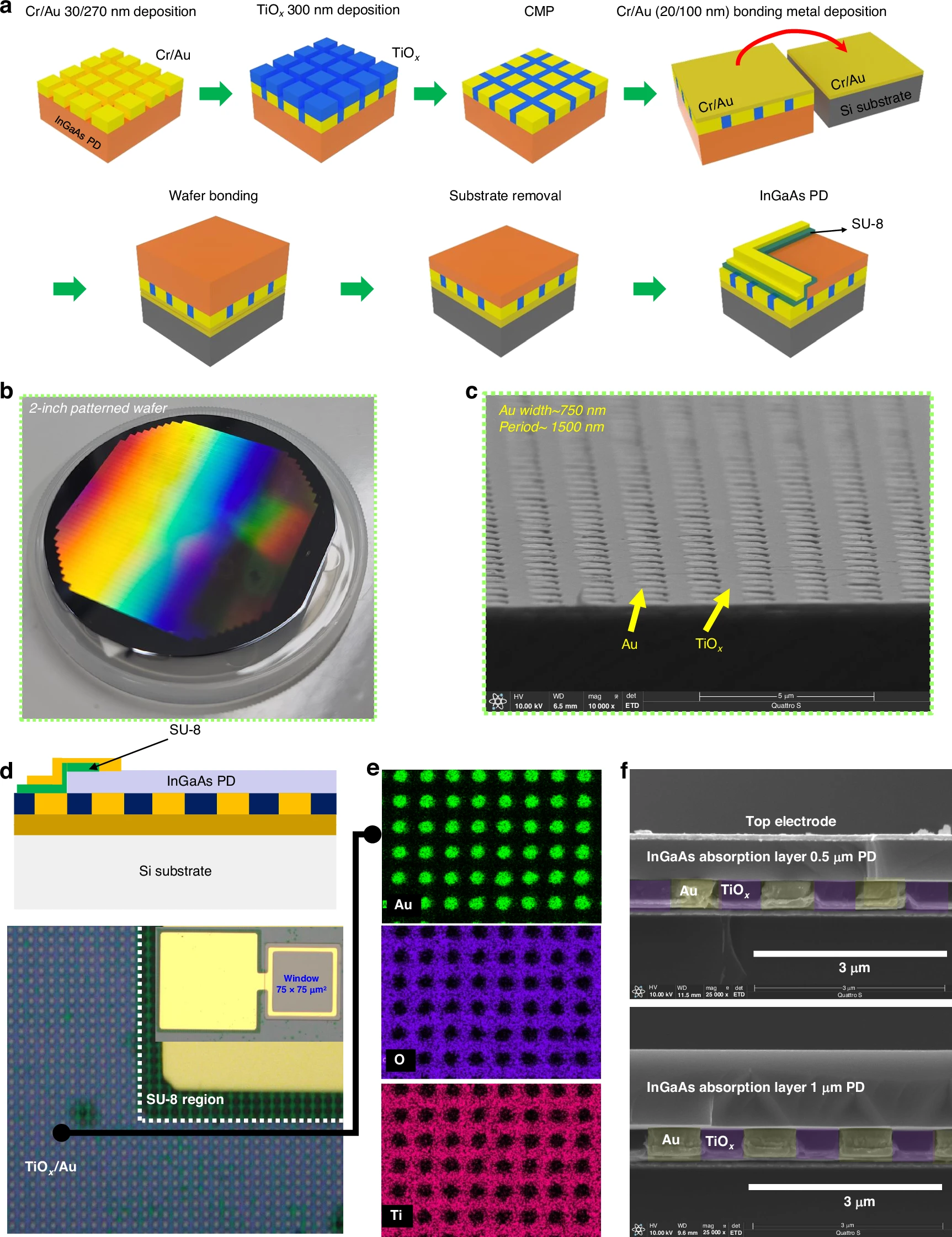
a Schematics of the GMR integrated InGaAs PDs by utilizing wafer bonding based thin film transfer method b Photograph of wafer-level patterned GMR structure with 1.5 μm period. c SEM image for periodic patterns consisting of Au width of 0.75 μm and TiOx 0.75 μm. d Schematic image of the fabricated PD on GMR structure and optical image of fabricated devices. e EDX images of Ti, O, and Au atoms at the top view. f Fabricated 0.5 μm and 1.0 μm AL InGaAs PD on GMR Si structure

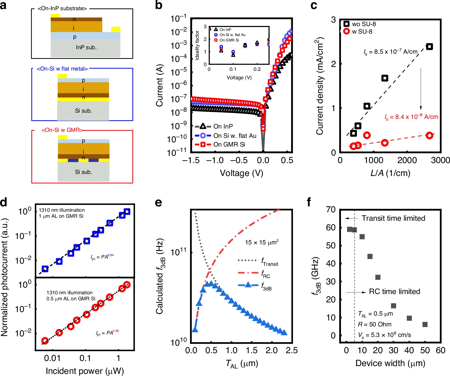
a Schematics of the fabricated device structures with different bottom structures. b I–V characteristics for 1.0 μm AL InGaAs PD on InP, flat metal, GMR, and ideality factors as an inset figure (c) Surface leakage currents for 1 μm AL InGaAs PD with/without SU-8 passivation using size dependency. d Iph–Pin characteristics for 0.5 and 1 μm AL PDs on GMR Si. e Calculated f3dB for 15 × 15 μm2 devices in terms of TAL. f Calculated f3dB as a function of device width to confirm the transit time limited bandwidth


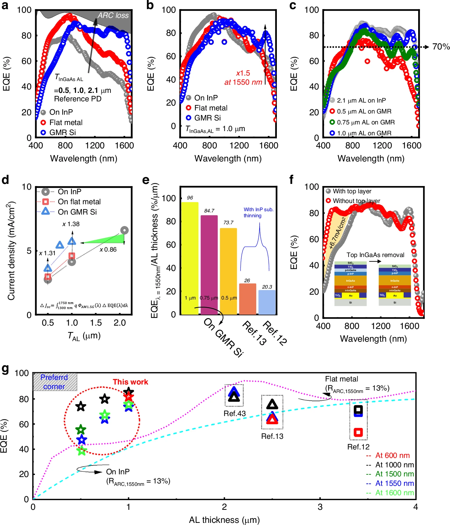
a EQE spectra for fabricated PDs on InP substrate with different TAL. b EQE spectra for fabricated 1 μm AL PDs on different bottom structures. c Resulting EQE spectra for different TAL on GMR structure and reference 2.1 μm AL PDs on InP substrate. d Calculated current density using EQE spectrum as a function of TAL and structures. e Comparison of normalized performances of EQE per TAL for proposed devices and conventional PDs. f Fabricated devices with/without 20 nm surface InGaAs layer for 1 μm AL PDs on GMR Si. g Benchmark for state-of-the-art InGaAs-based SWIR pixels with simulated EQE lines as a function of TAL variation (Dashed line: InGaAs PD on InP substrate, dotted line: InGaAs PD on flat metal structure, with the same ARC of this experiment)


Full text:  https://www.nature.com/articles/s41377-024-01652-6

Monday, December 16, 2024

SPAD camera for diffuse correlation spectroscopy

In a paper titled "ATLAS: a large array, on-chip compute SPAD camera for multispeckle diffuse correlation spectroscopy" in Biomedical Optics Express, Alistair Gorman et al. of University of Edinburgh write:

Abstract: We present ATLAS, a 512 × 512 single-photon avalanche diode (SPAD) array with embedded autocorrelation computation, implemented in 3D-stacked CMOS technology, suitable for single-photon correlation spectroscopy applications, including diffuse correlation spectroscopy (DCS). The shared per-macropixel SRAM architecture provides a 128 × 128 macropixel resolution, with parallel autocorrelation computation, with a minimum autocorrelation lag-time of 1 µs. We demonstrate the direct, on-chip computation of the autocorrelation function of the sensor, and its capability to resolve changes in decorrelation times typical of body tissue in real time, at long source-detector separations similar to those achieved by the current leading optical modalities for cerebral blood flow monitoring. Finally, we demonstrate the suitability for in-vivo measurements through cuff-occlusion and forehead cardiac signal measurements.

Fig. 1. (a) Sensor chip micrograph. (b) Dark count rate per SPAD cumulative distribution. (c) Photon detection efficiency.


Fig. 2. (a) Macropixel layout and (b) Sensor architecture showing the column normalization processor which multiplies each macropixel autocorrelation sample Aτ by the number of BinClk cycles (N) and divides by the square of the total photon count (Cτ0)2 before summing each entire row in a pipelined adder.


  Fig. 3. Macropixel signal flow diagram. 5-bit photon counts Cτ0 from the SPAD are delayed progressively 31 times, multiplied by the current value of Cτi and accumulated as Aτ. The autocorrelation calculation of g2(τ) needs to be normalized by (Cτ0)2/Tint.


 Fig. 4. Macropixel circuit block diagram. This shows the hardware implementation of Fig. 3. 16 SPADs are OR-ed and counted in a 5-bit accumulator. A 31 stage 5-bit shift register creates delayed photon counts at BinClk rate. A shared multiplier multiplexed operating at 32 times higher frequency (PixClk) generates the Aτ samples in an 32 × 22b SRAM.

Fig. 5. Macropixel timing diagram. In each BinClk period photon counts are delayed and shifted one place in the 5-b shift register. In that time PixClk initiates 32 10-b multiply and add (precharge, modify write) operations around each word location in the 32 × 22b SRAM.


 Fig. 6. (a) Target for verification of autocorrelation imaging mode. Example autocorrelations from the highlighted pixels in (a), corresponding to frequencies of 390.6 kHz (b) and 97.7 kHz (c).


 Fig. 7. (a) Measured and (b) theoretical normalized autocorrelations for frequencies between 12.2 and 195.3 kHz.


 Fig. 8. Autocorrelation image sequences with 10% duty cycle pulsed wave LED illumination of A and B targets. (a) Low frequency 8 kHz/4 kHz and 26 kHz/1 kHz pulsed wave images over a 1.28-12.8 µs lag range. (b) High frequency 96 kHz/112 kHz and 96 kHz/195 kHz pulsed wave images over an 8.96-20.48 µs lag range.


Fig. 9. (a) Ensemble average correlation calculated on-chip (blue) and off-chip (red). (b) Ensemble average SNR gain with respect to the single macropixel mean SNR at increasing number of pixels.


 Fig. 10. Time constants from exponential fitting of autocorrelation of LED sequences.


Fig. 11. Illustration of experimental setup to assess the sensitivity for DCS measurements.


  Fig. 12. (a) Measured optical power from the end of the detector fiber bundle at different source-detector separations on human forehead. (b) Typical range of time constants measured from adult forehead from exponential fitting of autocorrelations acquired with ATLAS in ensemble mode, with a 10 mm source detector separation and an integration time of 13.1 ms (8192 iterations) per sample. (c) Time series of time constant from exponential fitting of autocorrelations acquired with ATLAS in ensemble mode, from a rotating PLA disc (Fig. 11), driven with a square wave voltage to produce a similar range of time constants as measured from the forehead.

Fig. 13. Normalized time series of relative time constant from exponential fit, and best fit square wave.
 

Fig. 14. MAE against distal fiber powers between 3 and 30 nW.
 

Fig. 15. (a) Source and detection fiber at palm. (b) Time constant during and after a linear increase of wrist occlusion pressure from 0 mm Hg to a peak of 165 mm Hg at 40 s. (c) Six pulse periods of the time constant post occlusion.


Fig. 16. Time constants from exponential fitting of autocorrelations measured from forehead, for separations between the source and fiber of 35, 40, 45 and 50 mm.

Full text: https://opg.optica.org/boe/fulltext.cfm?uri=boe-15-11-6499&id=561837


Friday, December 13, 2024

SPAD direct-time-of-flight pixel with correlation-assisted processing

In a paper titled "Correlation-Assisted Pixel Array for Direct Time of Flight", A. Morsy and M. Kuijk or Vrije Universiteit write:

Abstract
Time of flight is promising technology in machine vision and sensing, with an emerging need for low power consumption, a high image resolution, and reliable operation in high ambient light conditions. Therefore, we propose a novel direct time-of-flight pixel using the single-photon avalanche diode (SPAD) sensor, with an in-pixel averaging method to suppress ambient light and detect the laser pulse arrival time. The system utilizes two orthogonal sinusoidal signals applied to the pixel as inputs, which are synchronized with a pulsed laser source. The detected signal phase indicates the arrival time. To evaluate the proposed system’s potential, we developed analytical and statistical models for assessing the phase error and precision of the arrival time under varying ambient light levels. The pixel simulation showed that the phase precision is less than 1% of the detection range when the ambient-to-signal ratio is 120. A proof-of-concept pixel array prototype was fabricated and characterized to validate the system’s performance. The pixel consumed, on average, 40 μW of power in operation with ambient light. The results demonstrate that the system can operate effectively under varying ambient light conditions and its potential for customization based on specific application requirements. This paper concludes by discussing the system’s performance relative to the existing direct time-of-flight technologies, identifying their strengths and limitations.

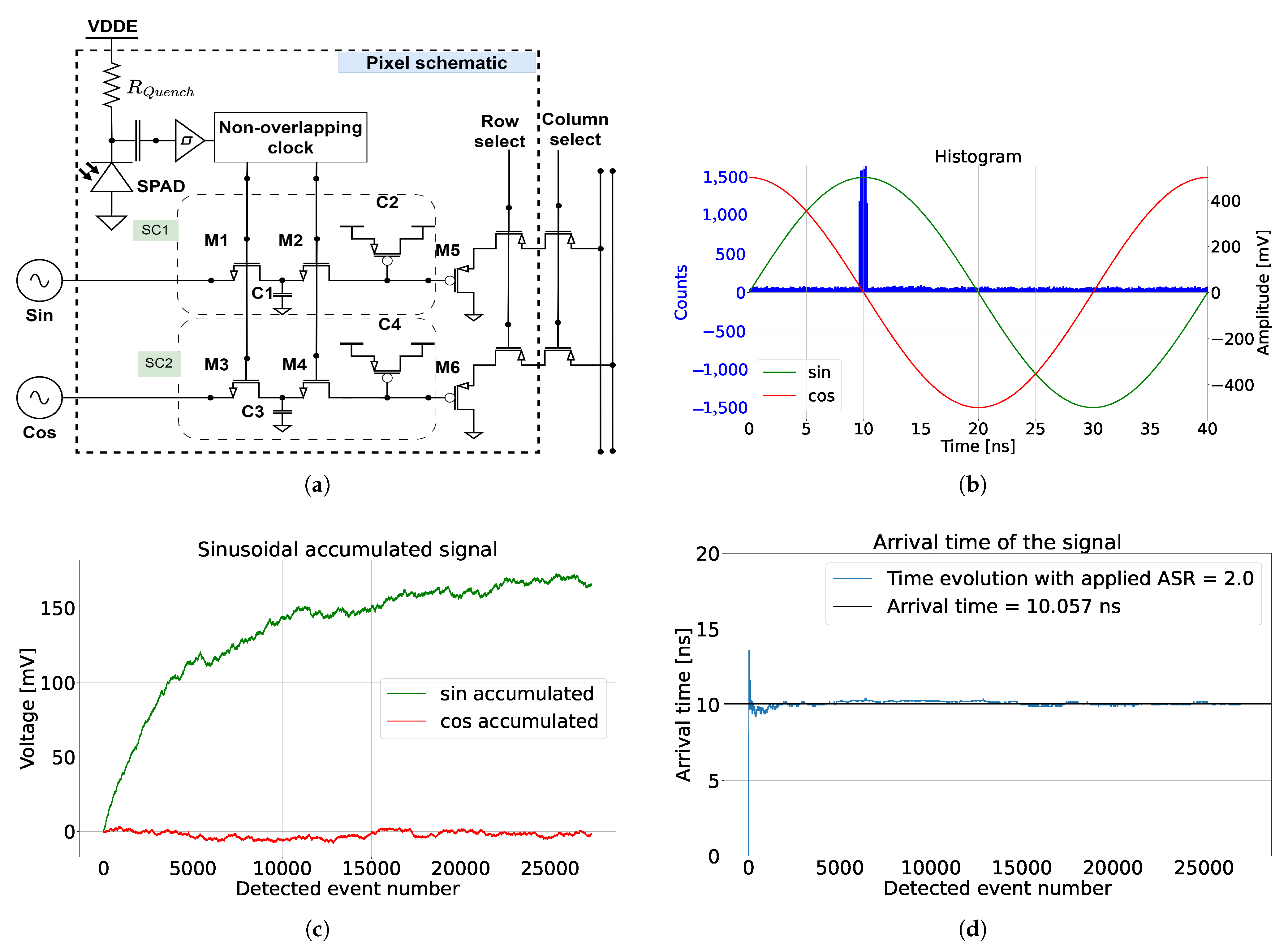
Figure 1. CA-dToF pixel schematic and simulation, where (a) is the pixel schematic and (b) is the histogram from the detected events. On the right side is the sinusoidal signals applied to the CA-dToF pixel, while (c) is the voltage evolution of the analog channels SC1 and SC2 and (d) is the calculated arrival time, with ASR = 2.


Figure 2. (a) Histogram of accumulated ambient light over a period {T} for a certain integration time. (b) Histogram of ambient light and laser pulses with an FWHM {a} detected with an arrival time {l} over a period {T}, along with ambient light that is uniformly distributed over the integration time.

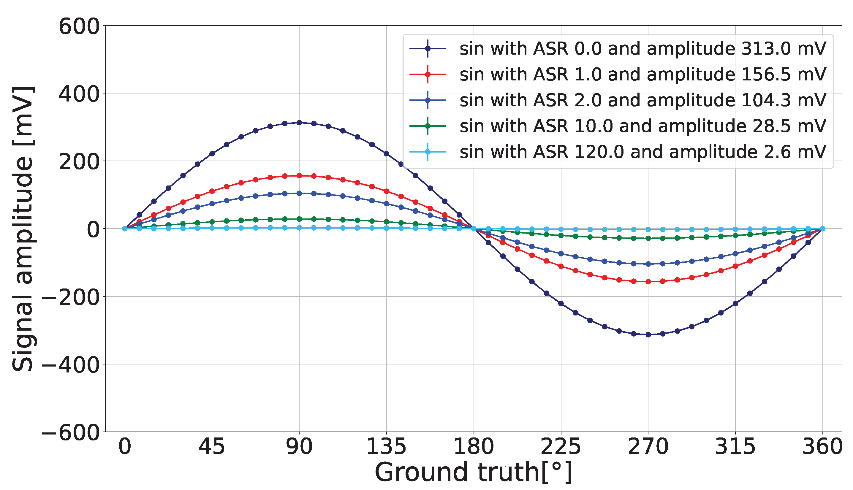
Figure 3. Reduction in the detected sine’s amplitude for different ASR values when a=4.25%·T and C=274.6 mV.

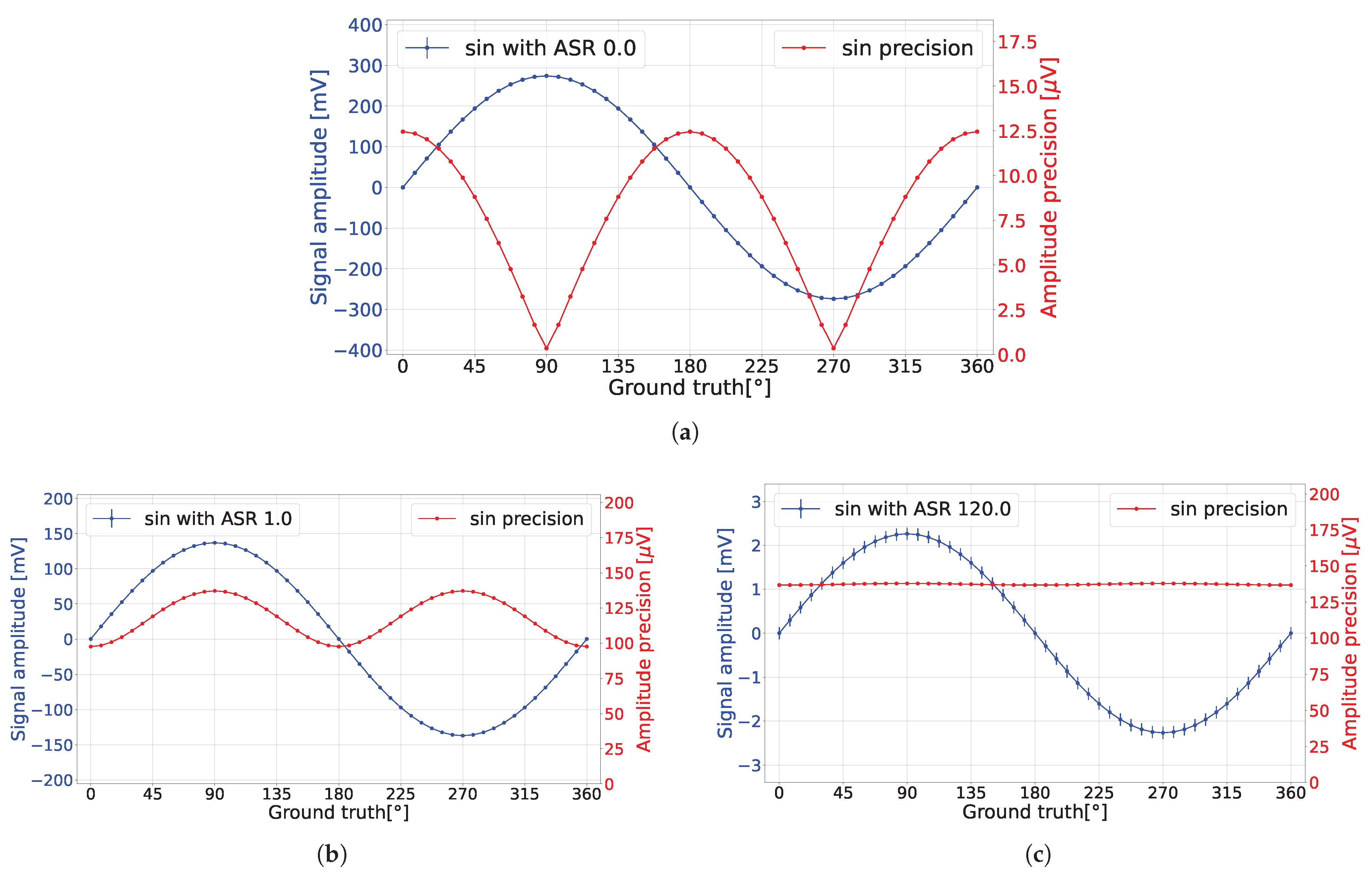
Figure 4. (a) When ASR = 0, the analytical model predicted that the detected voltage precision was oscillating due to active light shot noise. (b) When ASR = 1, the analytical model predicted that the detected voltage precision was oscillating due to the influence of laser and ambient light shot noise. (c) When ASR = 120, the analytical model predicted that the detected voltage precision oscillation was not significant due to the dominant ambient light shot noise.

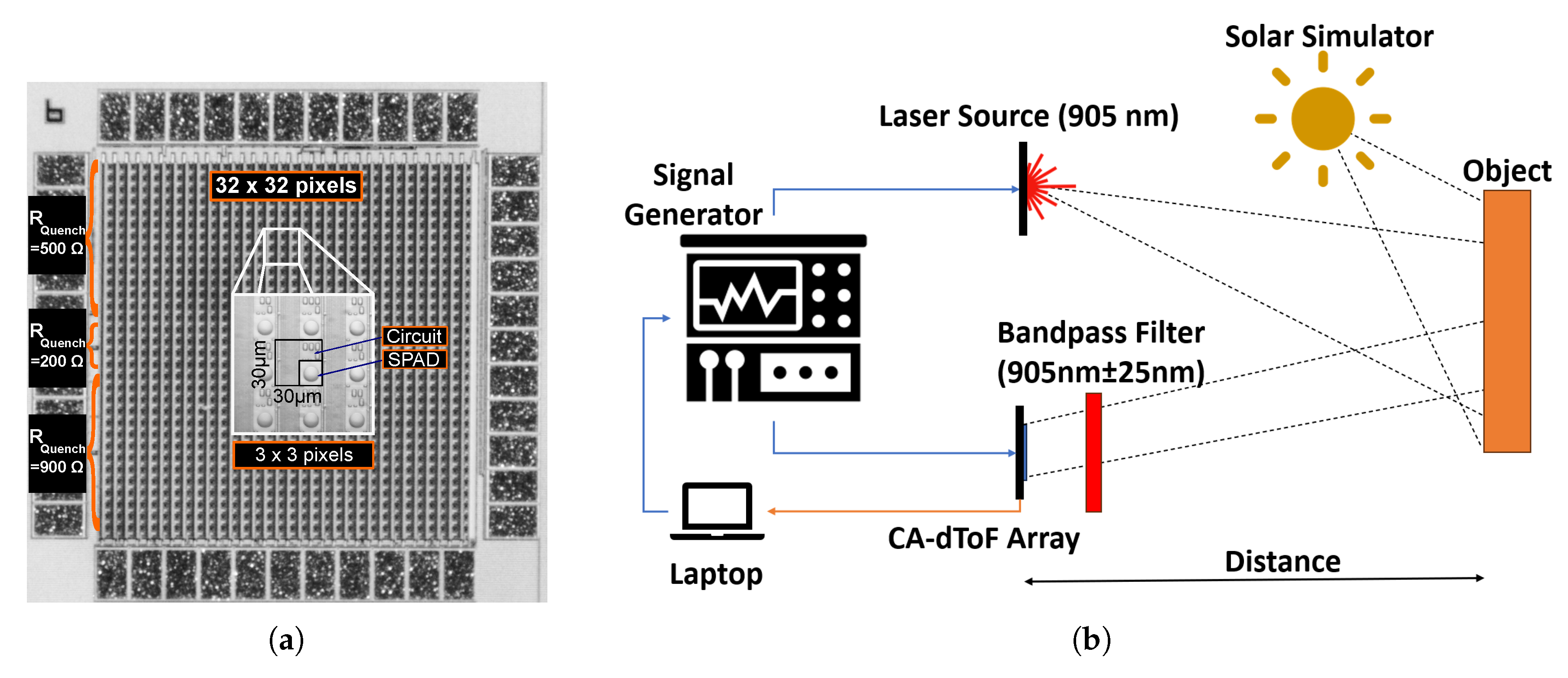
Figure 12. (a) CA-dToF pixel array micrograph with three different quenching resistors. (b) The experimental set-up.

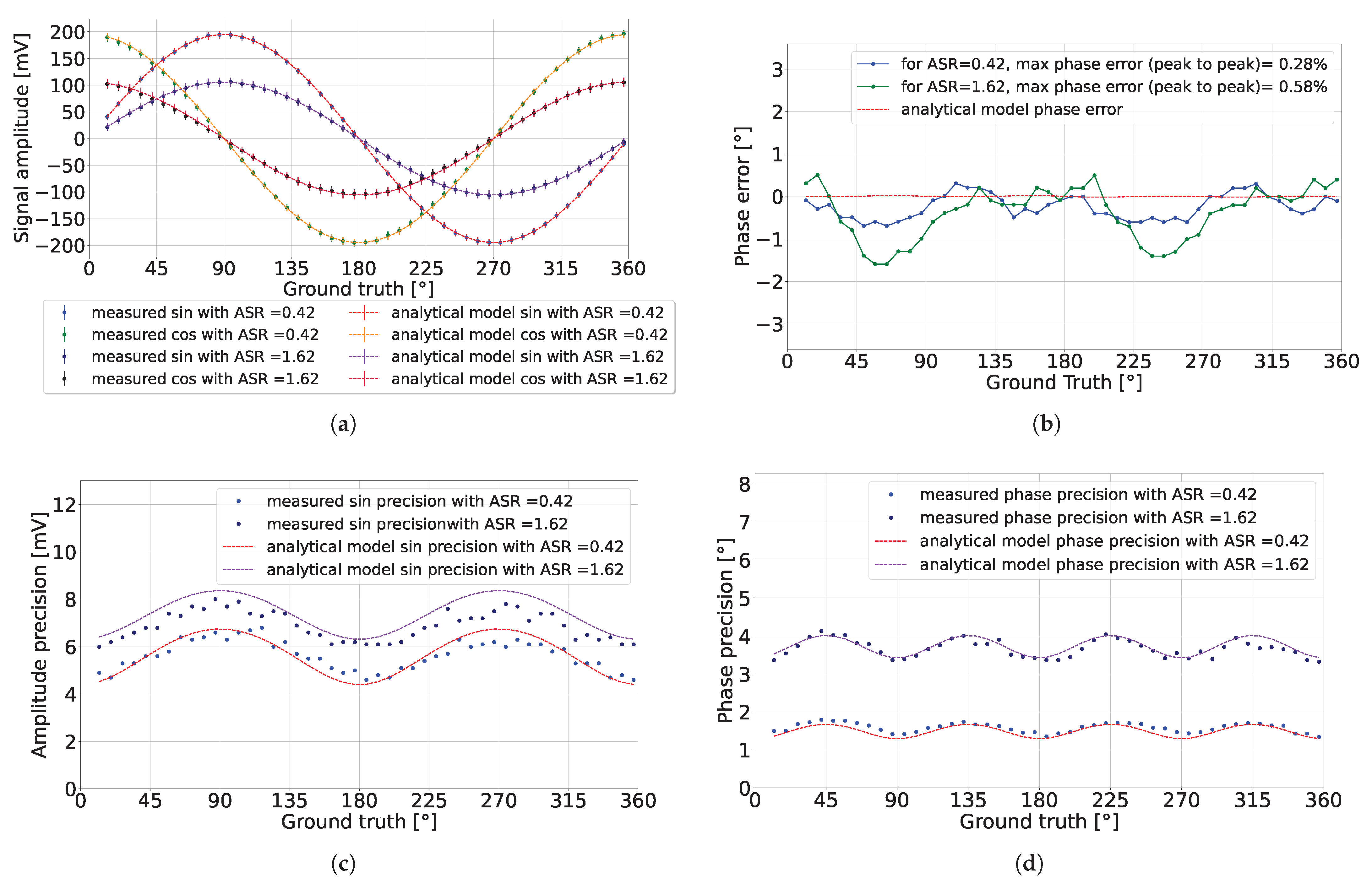
Figure 13. CA-dToF pixel experimental results for two different ASR values: (a) detected signal, (b) detected phase error, (c) detected amplitude precision, and (d) detected phase precision.

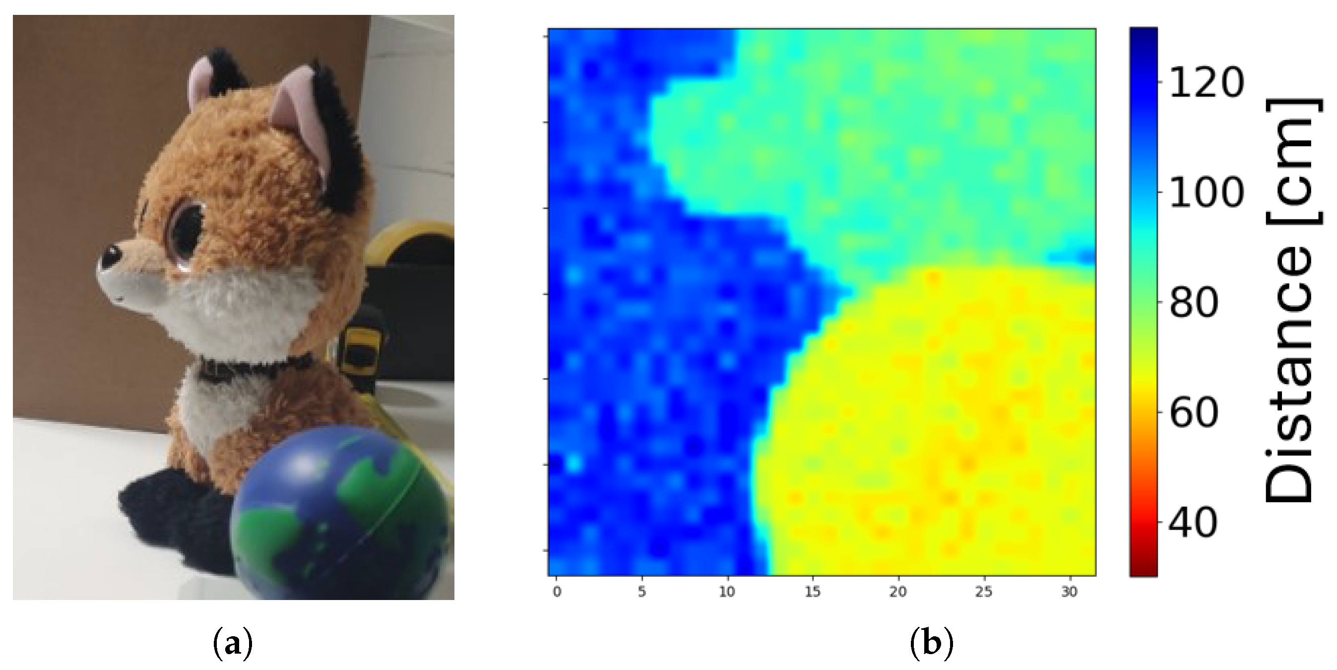
Figure 15. A snapshot of a scene with the 32×32 pixel array at the room’s ambient light. (a) Colored image of the scene. (b) The 3D image.


Full text: https://www.mdpi.com/1424-8220/24/16/5380

Wednesday, December 11, 2024

SK Hynix CIS business reorg

SK Hynix restructures CIS organization seemingly to replicate HBM success model

Link: https://www.digitimes.com/news/a20241210PD215/sk-hynix-cis-hbm-business-market.html

Despite the low profitability of SK Hynix's CMOS image sensor (CIS) business, the company has decided to retain this segment and reorganize its CIS development team under the Future Technology Research Institute, possibly hoping to replicate the successful narrative seen in high bandwidth memory (HBM).
According to industry sources cited by ZDNet Korea, SK Hynix CTO Seon-Yong Cha is expected to also lead CIS development.

Some analysts believe that SK Hynix endured a period of poor profitability in its HBM business but ultimately achieved success in the artificial intelligence (AI) chip market. In the future, demand for SK Hynix's CIS products may extend beyond the smartphone sector to include automotive, machine vision, and industrial markets.

Compared to other sectors within SK Hynix, the CIS business has lower profitability. Coupled with a shrinking smartphone market in recent years, there has been a decline in CIS demand, making it challenging for SK Hynix to secure a leading position in the CIS market.
According to market research firm Yole Développement, the top three players in the CIS market in 2023 are Sony with 45% market share, Samsung Electronics (Samsung) with 19%, and OmniVision with 11%. Meanwhile, SK Hynix ranks sixth with only 4% market share.

SK Hynix plans to transfer most of its CIS developers to other business units in 2024, resulting in a reduction of CIS production capacity by more than half compared to 2023. There was speculation within the South Korean industry that SK Hynix might "abandon the CIS business," but the company ultimately decided to continue its operations in this area.

SK Hynix president Noh-Jung Kwak reportedly has a strong desire to develop the CIS business. During a regular shareholders' meeting in March 2024, Kwak stated that he does not intend to abandon the CIS business, acknowledging both strengths and weaknesses compared to competitors while stressing that SK Hynix is analyzing these factors.

SK Hynix acquired the CIS development company SiliconFile in 2008, marking its entry into the CIS market. The absorption of SiliconFile in 2014 marked the beginning of its expansion in the CIS field. By 2019, SK Hynix established a CIS R&D center in Japan and launched the CIS brand Black Pearl.
SK Hynix previously supplied CIS components to mid-range Chinese smartphones and successfully provided sensors for Samsung's foldable Galaxy Z Fold3/Flip3 series and Galaxy A series in 2021.

Friday, December 06, 2024

Event cameras for GPS-free drone navigation

Link: https://spectrum.ieee.org/drone-gps-alternatives

A recent article in IEEE Spectrum titled "Neuromorphic Camera Helps Drones Navigate Without GPS High-end positioning tech comes to low-cost UAVs" discusses efforts in using neuromorphic cameras to achieve GPS-free navigation for drones.

Some excerpts:

[GPS] signals are vulnerable to interference from large buildings, dense foliage, or extreme weather and can even be deliberately jammed. [GPS-free navigation systems that rely only on] accelerometers and gyroscopes [suffer from] errors [that] accumulate over time and can ultimately cause a gradual drift. ... Visual navigation systems  [consume] considerable computing and data resources.

A pair of navigation technology companies has now teamed up to merge the approaches and get the best of both worlds. NILEQ, a subsidiary of British missile-maker MBDA based in Bristol, UK, makes a low-power visual navigation system that relies on neuromorphic cameras. This will now be integrated with a fiber optic-based INS developed by Advanced Navigation in Sydney, Australia, to create a positioning system that lets low-cost drones navigate reliably without GPS.

[...]

[Their proprietary algorithms] process the camera output in real-time to create a terrain fingerprint for the particular patch of land the vehicle is passing over. This is then compared against a database of terrain fingerprints generated from satellite imagery, which is stored on the vehicle. [...]

The companies are planning to start flight trials of the combined navigation system later this year, adds Shaw, with the goal of getting the product into customers hands by the middle of 2025.

Wednesday, December 04, 2024

Quantum Solutions announces SWIR camera based on quantum dot technology

Link: https://quantum-solutions.com/product/q-cam-swir-camera/#description

Oxford, UK – November 26, 2024 – Quantum Solutions proudly announces the release of the Q.Cam™ , an advanced Short-Wave Infrared (SWIR) camera designed for outdoor applications.

Redefining SWaP for Outdoor Applications:
The Q.Cam™ ™ sets a new standard for low Size, Weight, and Power (SWaP) in SWIR cameras, making it ideal for outdoor applications where space is limited and visibility in challenging conditions like smoke, fog, and haze is crucial.

Developed in collaboration with a leading partner, the Q.Cam™ is the first USB 3.0 camera featuring Quantum Solutions’ state-of-the-art Quantum Dot SWIR sensor, offering VGA resolution (640 x 512 pixels) with a wide spectral range of 400 nm to 1700 nm.

The Q.Cam™ is incredibly compact, weighing only 35 grams with dimensions of 35 x 25 x 25 mm³, making it perfect for integration in space-constrained environments. Its TEC-less design minimizes power consumption to an impressive <1.3 Watts, ideal for battery-powered operation.

Overcoming Outdoor Challenges:
Using SWIR cameras outdoors has traditionally been challenging due to varying lighting conditions and temperature-related image quality fluctuations requiring re-calibration of the camera to adjust to changing conditions. The Q.Cam™ addresses these issues with its advanced image correction technology, which automatically adjusts for factors like gain, temperature offset, and illumination. The camera can perform more than150+ automatic calibrations on the fly, ensuring consistent, high-quality images even in challenging and constantly changing outdoor environments. This advanced correction capability enables a TEC-less design, significantly reducing power consumption without compromising image quality.


The integration of proprietary Quantum Dot technology allows Quantum Solutions to offer the Q.Cam™ as a cost-effective and accessible solution for bringing SWIR imaging to a wider range of outdoor applications.

Seamless Integration and Flexibility:
The Q.Cam™ comes equipped with a user-friendly USB 3.0 interface, a Graphical User Interface (GUI), and Python scripts for easy integration and control.

ITAR-Free and Ready for Global Deployment:
The Q.Cam™ is an ITAR-free product with a short lead time of 3 weeks, making it readily
available for global deployment in a variety of sectors, including:
• Security and Surveillance
• Defence
• Search and Rescue
• Environmental Monitoring
• Robotics and Machine Vision
• Automotive

Key Features of Q.Cam™ :
• Quantum Dot SWIR Sensor: 640 x 512 pixels, 400 nm - 1700 nm spectral range
• Best-in-class SWaP: 35 g, 35 x 25 x 25 mm³, <1.3 W power consumption
• Built-in Automatic Image Correction: Up to 150+ automatic image corrections
(Gain, Offset, Temperature, and Illumination)
• Cost-Effective and Accessible: Among the most affordable SWIR cameras
available in the market
• Frame Rate up to 60 Hz; Global Shutter
• Operating Temperature: -20°C to 50°C

Monday, December 02, 2024

Video of the Day: tutorial on iToF imagers


Abstract:
"Indirect Time of Flight 3D imaging is an emerging technology used in 3D cameras. The technology is based on measuring the time of flight of modulated light. It allows to generate fine grain depth images with several hundreds of thousand image points. I-TOF has become a standard solution for face recognition and authentication. Recently I-TOF is also used in various new applications, such as computational photography, gesture recognition and robotics. This talk will introduce the basic operation principle of an I-TOF 3D imager IC. The integrated building blocks will be discussed and the analog operation of an I-TOF pixel will be addressed in detail. System level topics of the camera module will also be covered to provide a complete overview of the technology."
This presentation was recorded as part of the lecture "Selected Topics of Advanced Analog Chip Design" from the Institute of Electronics at TU Graz.
Special thanks to Dr. Timuçin Karaca, for the insightful presentation.