[Jan 23, 2025: post title updated for clarity.]
In a paper titled "Highly-efficient (>70%) and Wide-spectral (400–1700 nm)
sub-micron-thick InGaAs photodiodes for future high-resolution image
sensors" in Light: Science & Applications, Dae-Myeong Geum et al. from KAIST write:
Abstract: This paper demonstrates the novel approach of sub-micron-thick InGaAs broadband photodetectors (PDs) designed for high-resolution imaging from the visible to short-wavelength infrared (SWIR) spectrum. Conventional approaches encounter challenges such as low resolution and crosstalk issues caused by a thick absorption layer (AL). Therefore, we propose a guided-mode resonance (GMR) structure to enhance the quantum efficiency (QE) of the InGaAs PDs in the SWIR region with only sub-micron-thick AL. The TiOx/Au-based GMR structure compensates for the reduced AL thickness, achieving a remarkably high QE (>70%) from 400 to 1700 nm with only a 0.98 μm AL InGaAs PD (defined as 1 μm AL PD). This represents a reduction in thickness by at least 2.5 times compared to previous results while maintaining a high QE. Furthermore, the rapid transit time is highly expected to result in decreased electrical crosstalk. The effectiveness of the GMR structure is evident in its ability to sustain QE even with a reduced AL thickness, simultaneously enhancing the transit time. This breakthrough offers a viable solution for high-resolution and low-noise broadband image sensors.
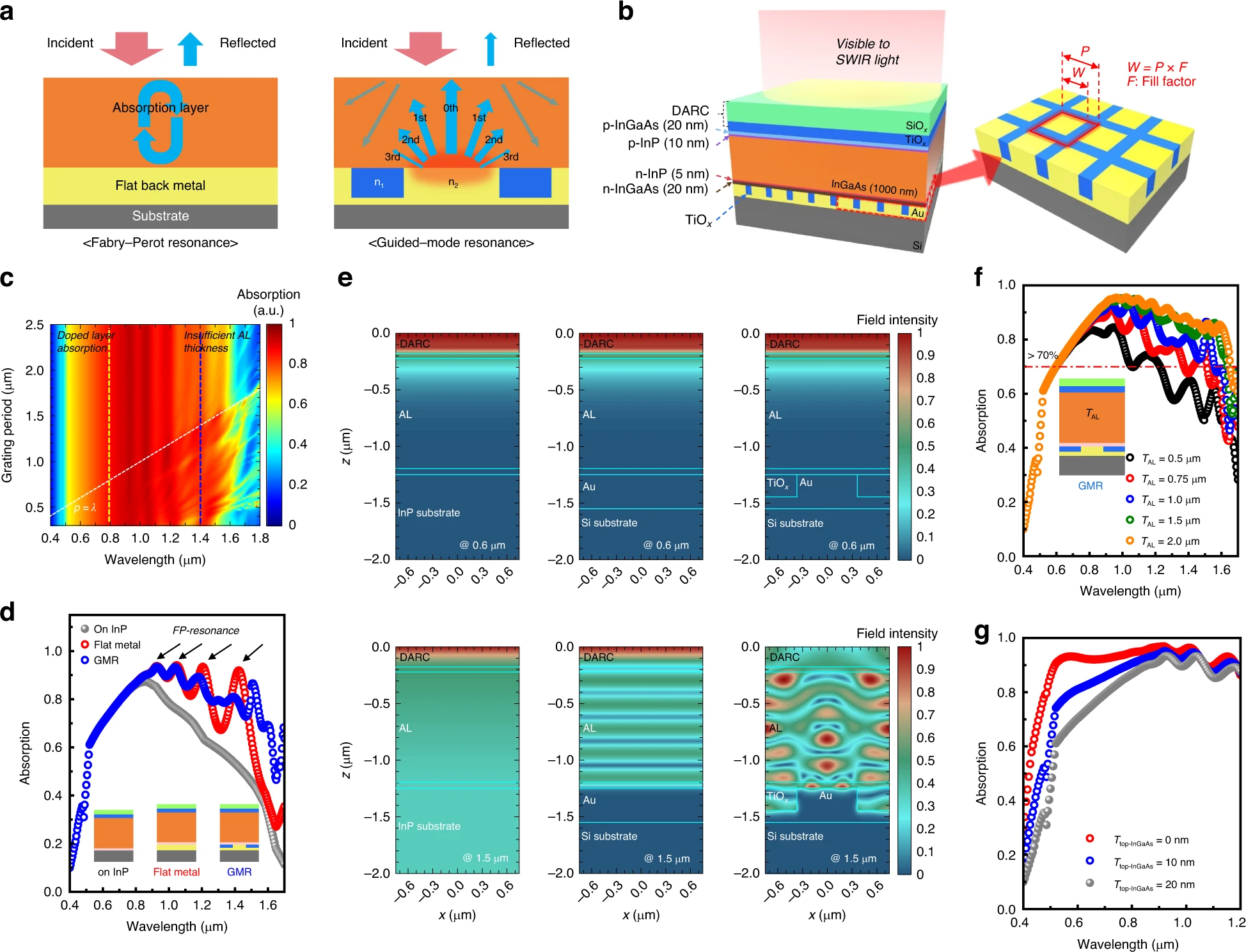
a Schematics of conventional Fabry-Perot resonance cavity and proposed GMR structure. b Design of GMR integrated InGaAs PD structures and design parameters of GMR structure. c 2D mapping results for the relative amount of absorption in AL grating period as a function of wavelength with fixed TAL = 1 μm. d RCWA simulation results with 1 μm AL PD on rear side engineering about InP substrate, flat metal structure, and GMR structure. e Electric field intensity distribution for 1.0 μm AL InGaAs PIN PDs on different bottom structures at 0.6 μm and 1.5 μm. f TAL dependent absorption spectra in terms of wavelength. g Top InGaAs layer thickness-dependent absorption spectra for visible light absorption
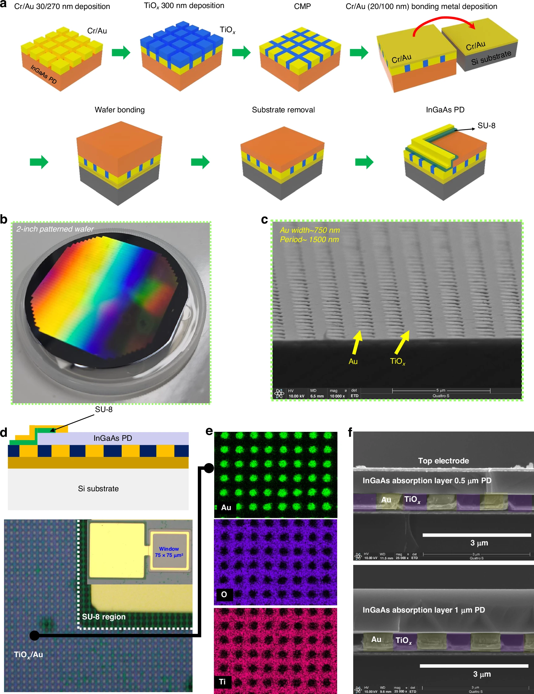
a Schematics of the GMR integrated InGaAs PDs by utilizing wafer bonding based thin film transfer method b Photograph of wafer-level patterned GMR structure with 1.5 μm period. c SEM image for periodic patterns consisting of Au width of 0.75 μm and TiOx 0.75 μm. d Schematic image of the fabricated PD on GMR structure and optical image of fabricated devices. e EDX images of Ti, O, and Au atoms at the top view. f Fabricated 0.5 μm and 1.0 μm AL InGaAs PD on GMR Si structure
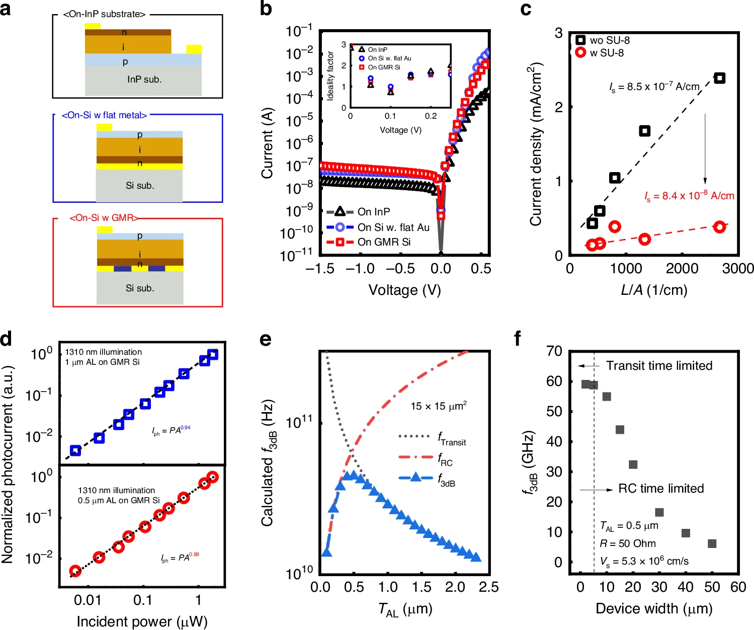
a Schematics of the fabricated device structures with different bottom structures. b I–V characteristics for 1.0 μm AL InGaAs PD on InP, flat metal, GMR, and ideality factors as an inset figure (c) Surface leakage currents for 1 μm AL InGaAs PD with/without SU-8 passivation using size dependency. d Iph–Pin characteristics for 0.5 and 1 μm AL PDs on GMR Si. e Calculated f3dB for 15 × 15 μm2 devices in terms of TAL. f Calculated f3dB as a function of device width to confirm the transit time limited bandwidth
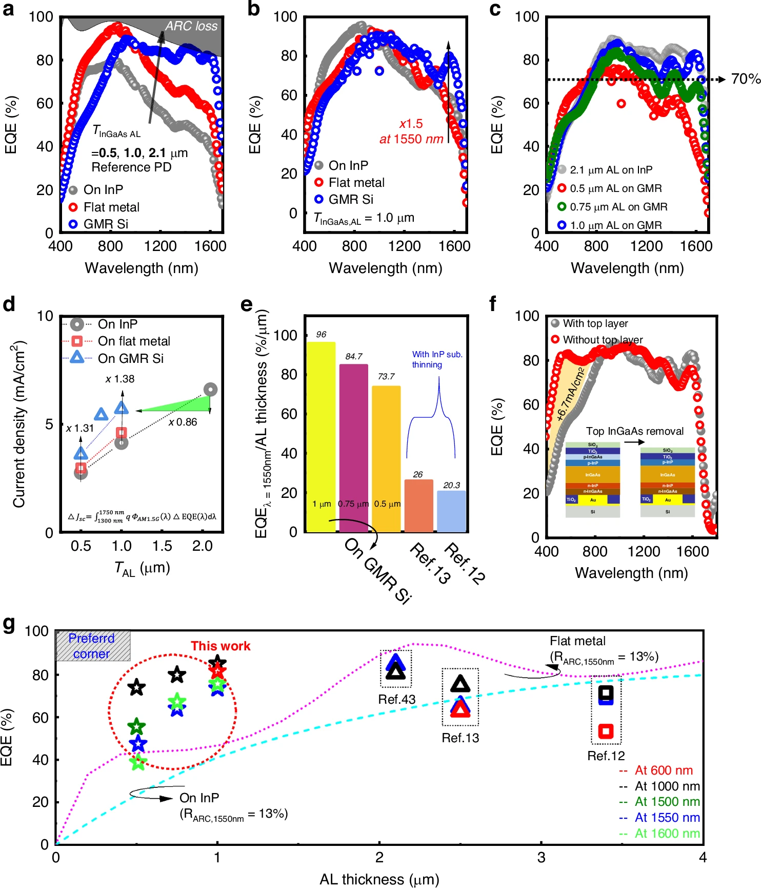
a EQE spectra for fabricated PDs on InP substrate with different TAL. b EQE spectra for fabricated 1 μm AL PDs on different bottom structures. c Resulting EQE spectra for different TAL on GMR structure and reference 2.1 μm AL PDs on InP substrate. d Calculated current density using EQE spectrum as a function of TAL and structures. e Comparison of normalized performances of EQE per TAL for proposed devices and conventional PDs. f Fabricated devices with/without 20 nm surface InGaAs layer for 1 μm AL PDs on GMR Si. g Benchmark for state-of-the-art InGaAs-based SWIR pixels with simulated EQE lines as a function of TAL variation (Dashed line: InGaAs PD on InP substrate, dotted line: InGaAs PD on flat metal structure, with the same ARC of this experiment)
Full text: https://www.nature.com/articles/s41377-024-01652-6


These are sub-micron-thick InGaAs photodiodes, not sub-micron pixels at all
ReplyDeleteCorrect, would be nice to correct the title..
DeleteBy the way what is the substrate thickness used in sub-micron pitch CMOS pixel please?
ReplyDeleteThanks!
ReplyDelete