A team from Stanford University's Laboratory for Integrated Nano-Quantum Systems (LINQS) and ArbabianLab present a new method that can potentially convert any conventional CMOS image sensor into an amplitude-modulated continuous-wave time-of-flight camera. The paper titled "Longitudinal piezoelectric resonant photoelastic modulator for efficient intensity modulation at megahertz frequencies" appeared in Nature Communications.
Intensity modulators are an essential component in optics for controlling free-space beams. Many applications require the intensity of a free-space beam to be modulated at a single frequency, including wide-field lock-in detection for sensitive measurements, mode-locking in lasers, and phase-shift time-of-flight imaging (LiDAR). Here, we report a new type of single frequency intensity modulator that we refer to as a longitudinal piezoelectric resonant photoelastic modulator. The modulator consists of a thin lithium niobate wafer coated with transparent surface electrodes. One of the fundamental acoustic modes of the modulator is excited through the surface electrodes, confining an acoustic standing wave to the electrode region. The modulator is placed between optical polarizers; light propagating through the modulator and polarizers is intensity modulated with a wide acceptance angle and record breaking modulation efficiency in the megahertz frequency regime. As an illustration of the potential of our approach, we show that the proposed modulator can be integrated with a standard image sensor to effectively convert it into a time-of-flight imaging system.
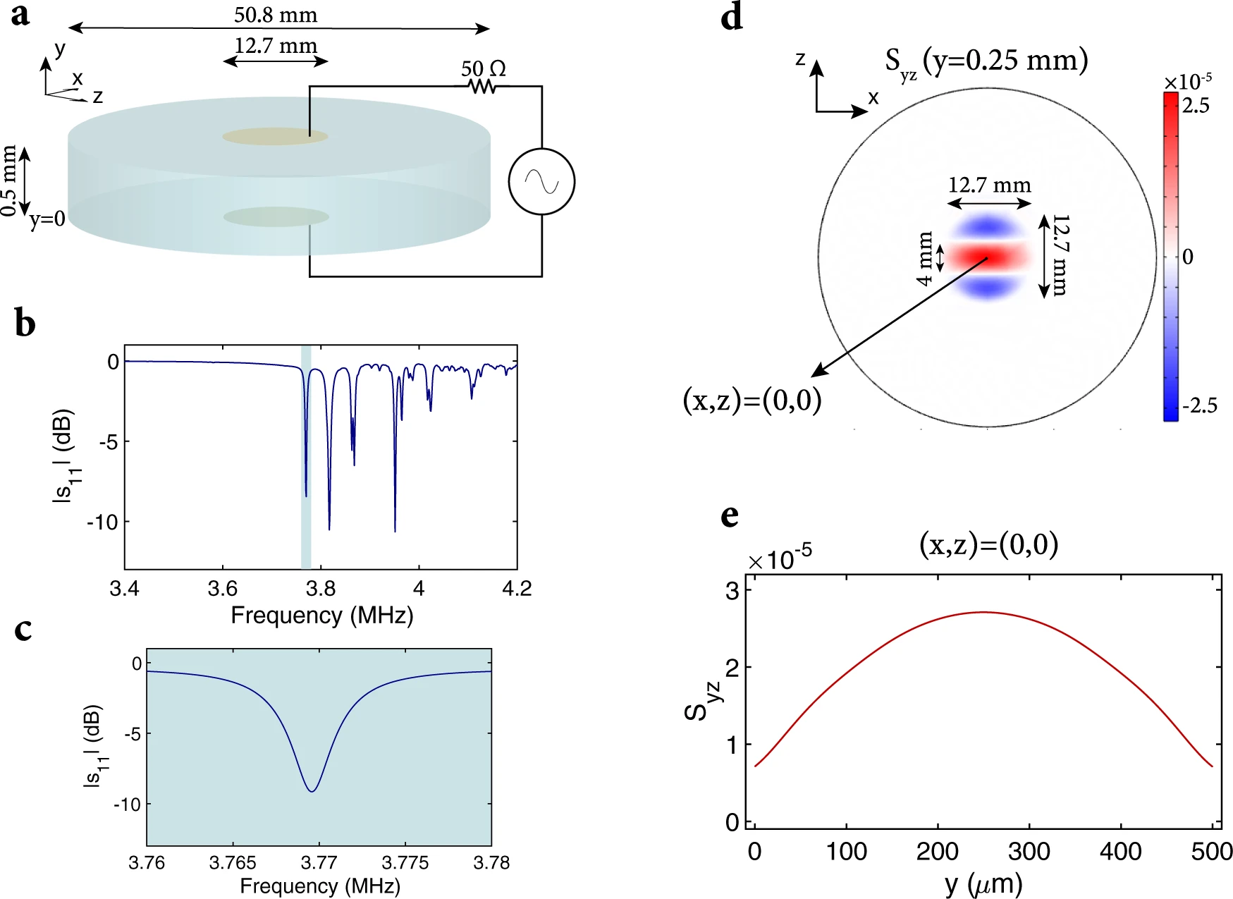
a) A Y-cut lithium niobate wafer of diameter 50.8 mm and of thickness 0.5 mm is coated on top and bottom surfaces with electrodes having a diameter of 12.7 mm. The wafer is excited with an RF source through the top and bottom electrodes. b) Simulated ∣s11∣ of the wafer with respect to 50 Ω, showing the resonances corresponding to different acoustic modes of the wafer (loss was added to lithium niobate to make it consistent with experimental results). The desired acoustic mode appears around 3.77 MHz and is highlighted in blue. c) The desired acoustic mode ∣s11∣ with respect to 50 Ω is shown in more detail. d) The dominant strain distribution (Syz) when the wafer is excited at 3.7696 MHz with 2 Vpp is shown for the center of the wafer. This strain distribution corresponds to the ∣s11∣ resonance shown in (c). e) The variation in Syz parallel to the wafer normal and centered along the wafer is shown when the wafer is excited at 3.7696 MHz with 2 Vpp.
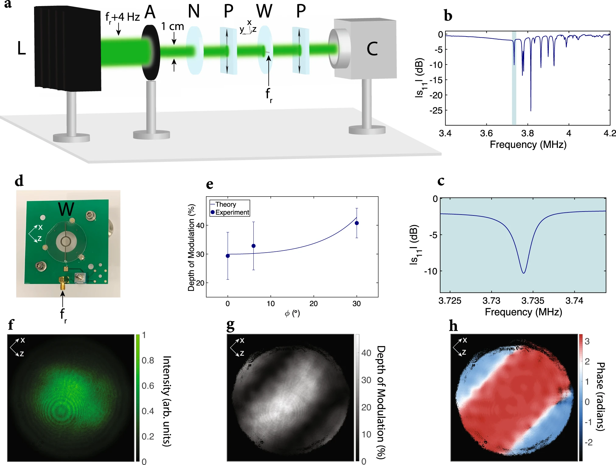
a) Schematic of the characterization setup is shown. The setup includes a laser (L) with a wavelength of 532 nm that is intensity-modulated at 3.733704 MHz, aperture (A) with a diameter of 1 cm, neutral density filter (N), two polarizers (P) with transmission axis t^=(a^x+a^z)/2–√, wafer (W), and a standard CMOS camera (C). The wafer is excited with 90 mW of RF power at fr = 3.7337 MHz, and the laser beam passes through the center of the wafer that is coated with ITO. The camera detects the intensity-modulated laser beam. b) The desired acoustic mode is found for the modulator by performing an s11 scan with respect to 50 Ω using 0 dBm excitation power and with a bandwidth of 100 Hz. The desired acoustic mode is highlighted in blue. c) The desired acoustic mode is shown in more detail by performing an s11 scan with respect to 50 Ω using 0 dBm excitation power with a bandwidth of 20 Hz. d) The fabricated modulator is shown. e) The depth of intensity modulation is plotted for different angles of incidence for the laser beam (averaged across all the pixels), where ϕ is the angle between the surface normal of the wafer and the beam direction k^ (see “Methods” for more details). Error bars represent the standard deviation of the depth of intensity modulation across the pixels. f) Time-averaged intensity profile of the laser beam detected by the camera is shown for ϕ = 0. g) The DoM at 4 Hz of the laser beam is shown per pixel for ϕ = 0. h) The phase of intensity modulation at 4 Hz of the laser beam is shown per pixel for ϕ = 0.
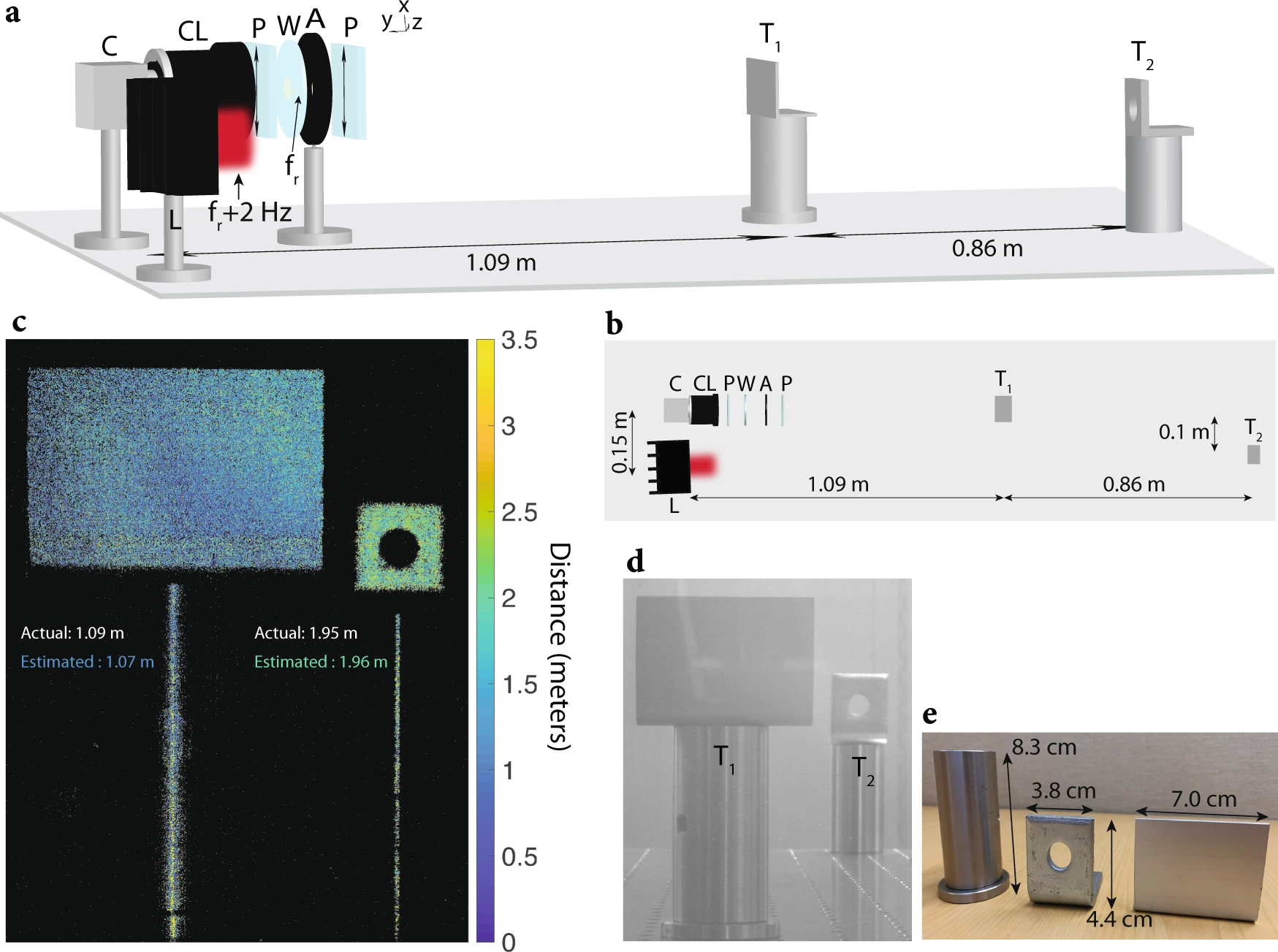
a) Schematic of the imaging setup is shown. The setup includes a standard CMOS camera (C), camera lens (CL), two polarizers (P) with transmission axis t^=(a^x+a^z)/sqrt(2), wafer (W), aperture (A) with a diameter of 4 mm, laser (L) with a wavelength of 635 nm that is intensity-modulated at 3.733702 MHz, and two metallic targets (T1 and T2) placed 1.09 m and 1.95 m away from the imaging system, respectively. For the experiment, 140 mW of RF power at fr = 3.7337 MHz is used to excite the wafer electrodes. The laser is used for illuminating the targets. The camera detects the reflected laser beam from the two targets, and uses the 2 Hz beat tone to extract the distance of each pixel corresponding to a distinct point in the scene (see “Methods” for more details). b) Bird’s eye view of the schematic in (a). c) Reconstructed depth map seen by the camera. Reconstruction is performed by mapping the phase of the beat tone at 2 Hz to distance using Eq. (3). The distance of each pixel is color-coded from 0 to 3 m (pixels that receive very few photons are displayed in black). The distance of targets T1 and T2 are estimated by averaging across their corresponding pixels, respectively. The estimated distances for T1 and T2 are 1.07 m and 1.96 m, respectively (averaged across all pixels corresponding to T1 and T2). d) Ambient image capture of the field-of-view of the camera, showing the two targets T1 and T2. e The dimensions of the targets used for ToF imaging are shown.
The paper points out limitations of other approaches such as spatial light modulators and meta-optics, but doesn't mention any potential challenges or limitations of their proposed method. Interestingly, the authors cite some recent papers on high-resolution SPAD sensors to make the claim that their method is more promising than "highly specialized costly image sensors that are difficult to implement with a large number of pixels." Although the authors do not explicitly mention this in the paper, their piezoelectric material of choice (lithium niobate) is CMOS compatible. Thin-film deposition of lithium niobate on silicon using a CMOS process seems to be an active area of research (for example, see Mercante et al., Optics Express 24(14), 2016 and Wang et al., Nature 562, 2018.)
No comments:
Post a Comment
All comments are moderated to avoid spam and personal attacks.