The AQUA research group at EPFL together with Global Foundries have published two new articles on 55 nm Bipolar-CMOS-DMOS (BCD) SPAD technology in the upcoming issues of IEEE Journal of Selected Topics in Quantum Electronics.
Engineering Breakdown Probability Profile for PDP and DCR Optimization in a SPAD Fabricated in a Standard 55 nm BCD Process
Link [open access article]: https://ieeexplore.ieee.org/stamp/stamp.jsp?tp=&arnumber=9543572
Abstract:
CMOS single-photon avalanche diodes (SPADs) have broken into the mainstream by enabling the adoption of imaging, timing, and security technologies in a variety of applications within the consumer, medical and industrial domains. The continued scaling of technology nodes creates many benefits but also obstacles for SPAD-based systems. Maintaining and/or improving upon the high-sensitivity, low-noise, and timing performance of demonstrated SPADs in custom technologies or well-established CMOS image sensor processes remains a challenge. In this paper, we present SPADs based on DPW/BNW junctions in a standard Bipolar-CMOS-DMOS (BCD) technology with results comparable to the state-of-the-art in terms of sensitivity and noise in a deep sub-micron process. Technology CAD (TCAD) simulations demonstrate the improved PDP with the simple addition of a single existing implant, which allows for an engineered performance without modifications to the process. The result is an 8.8 μ\mu m diameter SPAD exhibiting ∼\sim 2.6 cps/ μ\mu m 2^2 DCR at 20 ∘^{\circ} C with 7 V excess bias. The improved structure obtains a PDP of 62% and ∼\sim 4.2% at 530 nm and 940 nm, respectively. Afterpulsing probability is ∼\sim 0.97% and the timing response is 52 ps FWHM when measured with integrated passive quench/active recharge circuitry at 3 V excess bias.


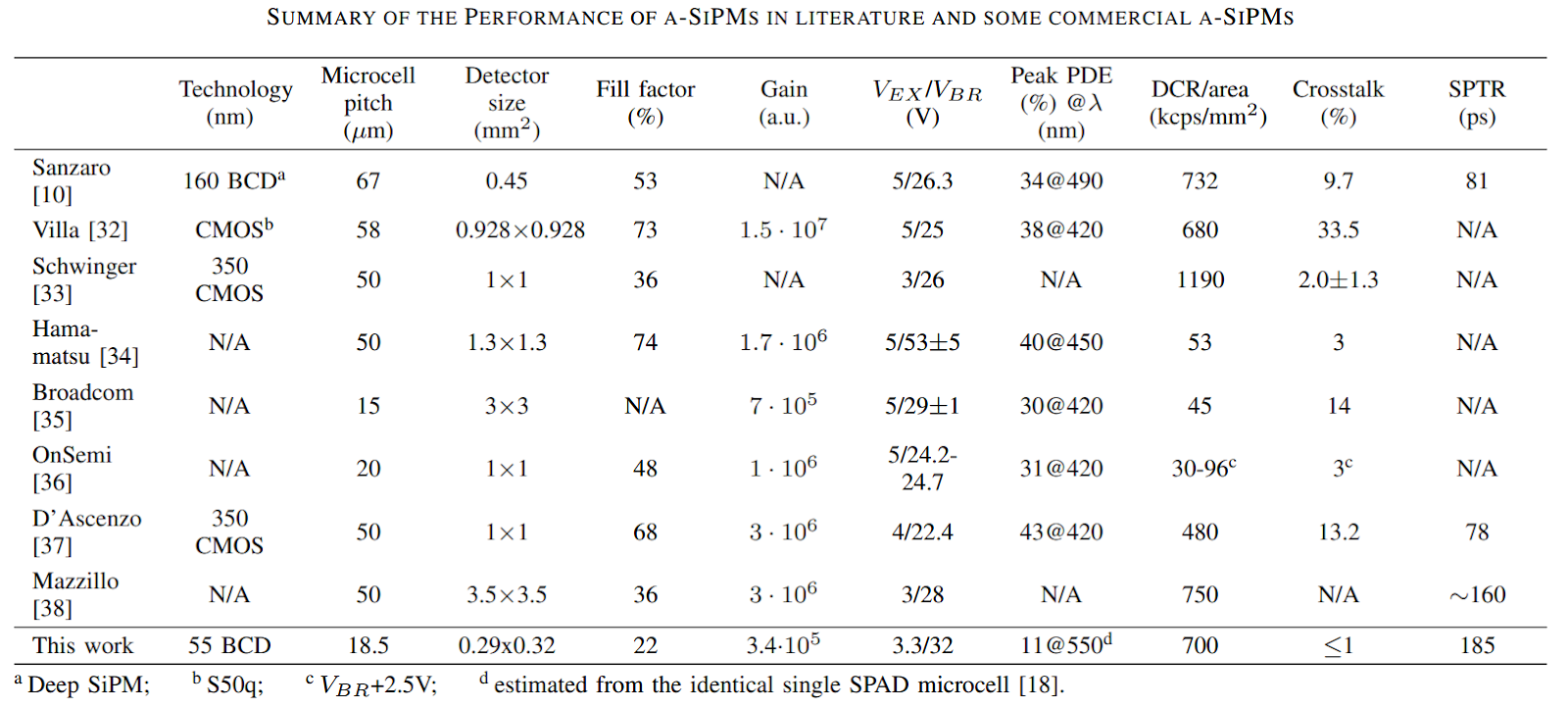
On Analog Silicon Photomultipliers in Standard 55-nm BCD Technology for LiDAR Applications
Link [subscription needed]: https://ieeexplore.ieee.org/document/9739982
Abstract:
We present an analog silicon photomultiplier (SiPM) based on a standard 55 nm Bipolar-CMOS-DMOS (BCD) technology. The SiPM is composed of 16 x 16 single-photon avalanche diodes (SPADs) and measures 0.29 x 0.32 mm2. Each SPAD cell is passively quenched by a monolithically integrated 3.3 V thick oxide transistor. The measured gain is 3.4 x 10⁵ at 5 V excess bias voltage. The single-photon timing resolution (SPTR) is 185 ps and the multiple-photon timing resolution (MPTR) is 120 ps at 3.3 V excess bias voltage. We integrate the SiPM into a co-axial light detection and ranging (LiDAR) system with a time-correlated single-photon counting (TCSPC) module in FPGA. The depth measurement up to 25 m achieves an accuracy of 2 cm and precision of 2 mm under the room ambient light condition. With co-axial scanning, the intensity and depth images of complex scenes with resolutions of 128 x 256 and 256 x 512 are demonstrated. The presented SiPM enables the development of cost-effective LiDAR system-on-chip (SoC) in the advanced technology.


No comments:
Post a Comment
All comments are moderated to avoid spam and personal attacks.