Researches from the Integrated Photonics Lab at UC-Berkeley recently published a paper titled "A large-scale microelectromechanical-systems-based silicon photonics LiDAR" proposing a CMOS-compatible high-resolution scanning MEMS LiDAR system.
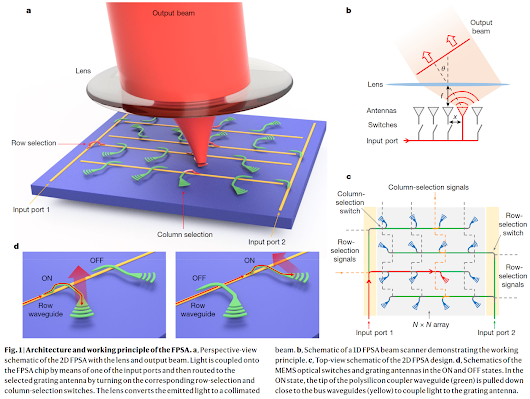
Three-dimensional (3D) imaging sensors allow machines to perceive, map and interact with the surrounding world. The size of light detection and ranging (LiDAR) devices is often limited by mechanical scanners. Focal plane array-based 3D sensors are promising candidates for solid-state LiDARs because they allow electronic scanning without mechanical moving parts. However, their resolutions have been limited to 512 pixels or smaller. In this paper, we report on a 16,384-pixel LiDAR with a wide field of view (FoV, 70° × 70°), a fine addressing resolution (0.6° × 0.6°), a narrow beam divergence (0.050° × 0.049°) and a random-access beam addressing with sub-MHz operation speed. The 128 × 128-element focal plane switch array (FPSA) of grating antennas and microelectromechanical systems (MEMS)-actuated optical switches are monolithically integrated on a 10 × 11-mm2 silicon photonic chip, where a 128 × 96 subarray is wire bonded and tested in experiments. 3D imaging with a distance resolution of 1.7 cm is achieved with frequency-modulated continuous-wave (FMCW) ranging in monostatic configuration. The FPSA can be mass-produced in complementary metal–oxide–semiconductor (CMOS) foundries, which will allow ubiquitous 3D sensors for use in autonomous cars, drones, robots and smartphones.


No comments:
Post a Comment
All comments are moderated to avoid spam and personal attacks.