A team from Military University of Technology (Poland) and Shanghai Institute of Technical Physics (China) have published a review article titled "Infrared avalanche photodiodes from bulk to 2D materials" in Light: Science & Applications journal.
Open access paper: https://www.nature.com/articles/s41377-023-01259-3
Abstract: Avalanche photodiodes (APDs) have drawn huge interest in recent years and have been extensively used in a range of fields including the most important one—optical communication systems due to their time responses and high sensitivities. This article shows the evolution and the recent development of AIIIBV, AIIBVI, and potential alternatives to formerly mentioned—“third wave” superlattices (SL) and two-dimensional (2D) materials infrared (IR) APDs. In the beginning, the APDs fundamental operating principle is demonstrated together with progress in architecture. It is shown that the APDs evolution has moved the device’s performance towards higher bandwidths, lower noise, and higher gain-bandwidth products. The material properties to reach both high gain and low excess noise for devices operating in different wavelength ranges were also considered showing the future progress and the research direction. More attention was paid to advances in AIIIBV APDs, such as AlInAsSb, which may be used in future optical communications, type-II superlattice (T2SLs, “Ga-based” and “Ga-free”), and 2D materials-based IR APDs. The latter—atomically thin 2D materials exhibit huge potential in APDs and could be considered as an alternative material to the well-known, sophisticated, and developed AIIIBV APD technologies to include single-photon detection mode. That is related to the fact that conventional bulk materials APDs’ performance is restricted by reasonably high dark currents. One approach to resolve that problem seems to be implementing low-dimensional materials and structures as the APDs’ active regions. The Schottky barrier and atomic level thicknesses lead to the 2D APD dark current significant suppression. What is more, APDs can operate within visible (VIS), near-infrared (NIR)/mid-wavelength infrared range (MWIR), with a responsivity ~80 A/W, external quantum efficiency ~24.8%, gain ~105 for MWIR [wavelength, λ = 4 μm, temperature, T = 10–180 K, Black Phosphorous (BP)/InSe APD]. It is believed that the 2D APD could prove themselves to be an alternative providing a viable method for device fabrication with simultaneous high-performance—sensitivity and low excess noise.
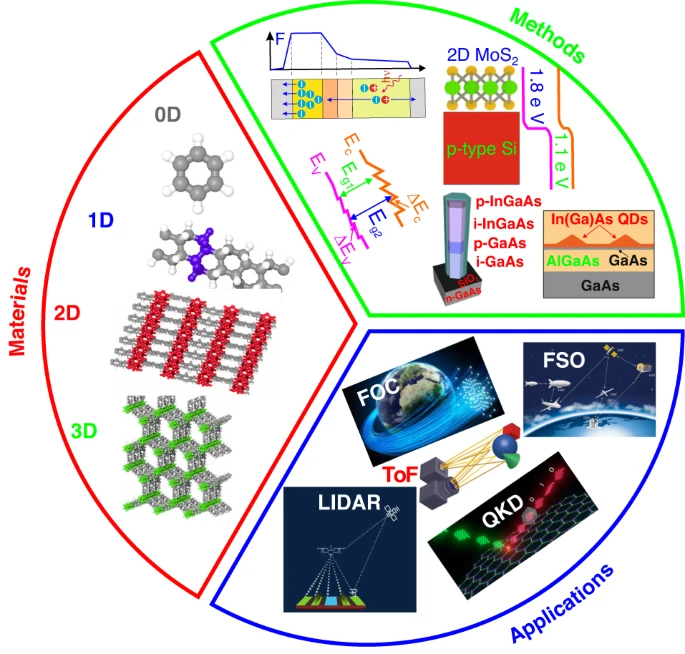
Fig. 1: Bulk to low-dimensional material, tactics to fabricate APDs and possible applications: FOC, FSO, LIDAR and QKDs.
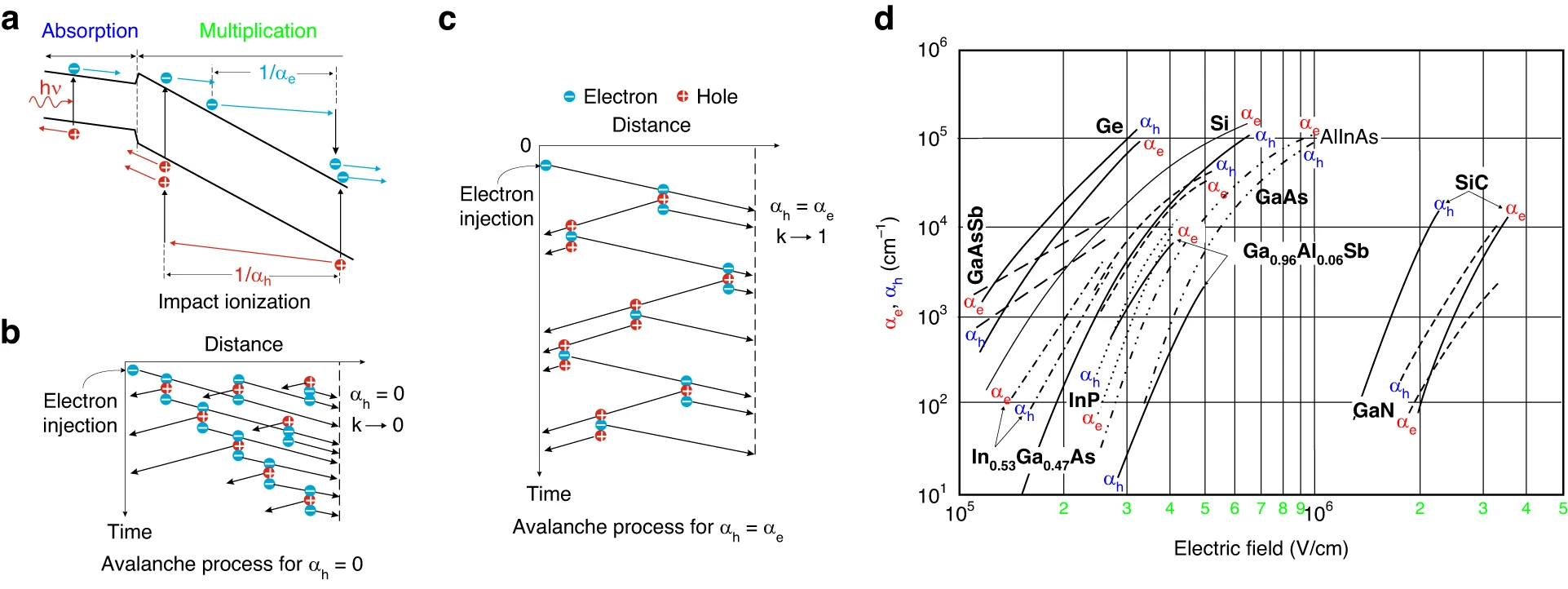
Fig. 2: The APD’s operating principle. a Electron and hole multiplication mechanisms, schematic of multiplication mechanism for b k = 0 (αh = 0) and c k = 1 (αe = αh), where k = αh/αe – αe, αh represent electron and hole multiplication coefficients. d αe, αh ionization coefficients versus electric field for selected semiconductors used for APDs’ fabrication
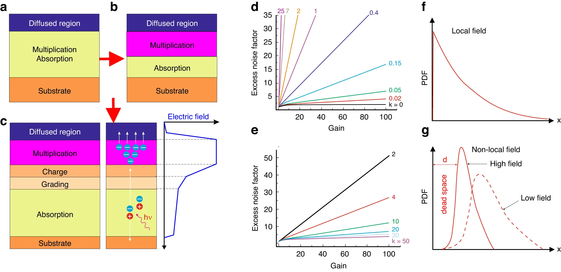
Fig. 3: APDs. a p–n device, b SAM device, and c SAGCM device with electric field distribution. F(M) dependence on M for the selected k = αh/αe in APDs when: d electrons and e holes dominate in the avalanche mechanism. The multiplication path length probability distribution functions in the: f local and g non-local field “dead space” models
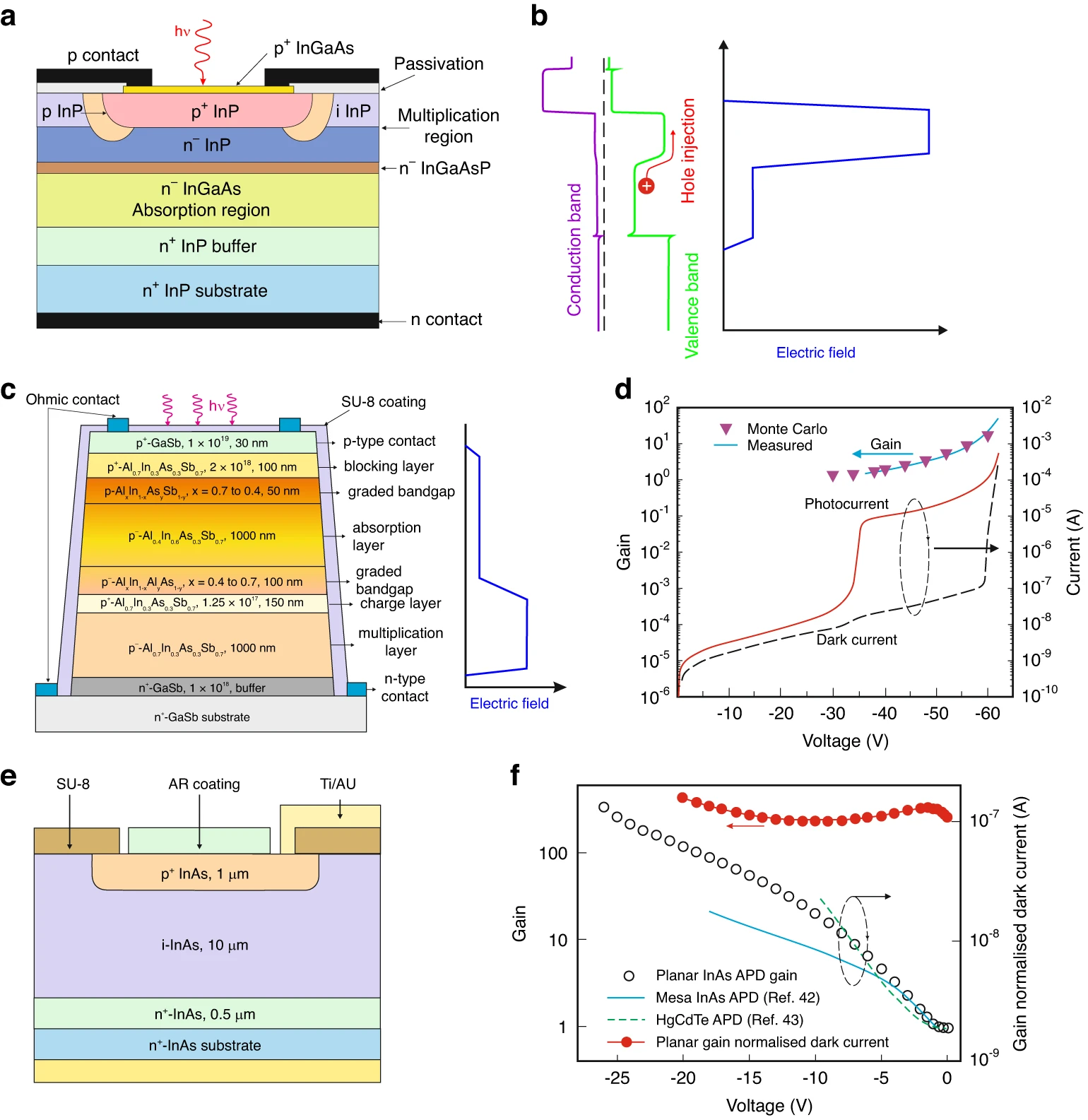
Fig. 4: InGaAs/InP SAM-APD. a device structure, b energy band profile, and electric field under normal reverse bias condition. AlxIn1–xAsySb1–y based SACM APD: c detector’s design with the E distribution within the detector, d measured and theoretically simulated gain, dark current, photocurrent versus reverse voltage for 90 μm diameter device at room temperature39. InAs planar avalanche photodiode: e a schematic design diagram, f comparison of the gain reached by 1550 nm wavelength laser132,133. The M normalized dark current for 100 μm radius planar APD was presented for 200 K
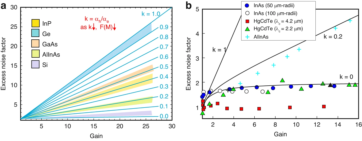
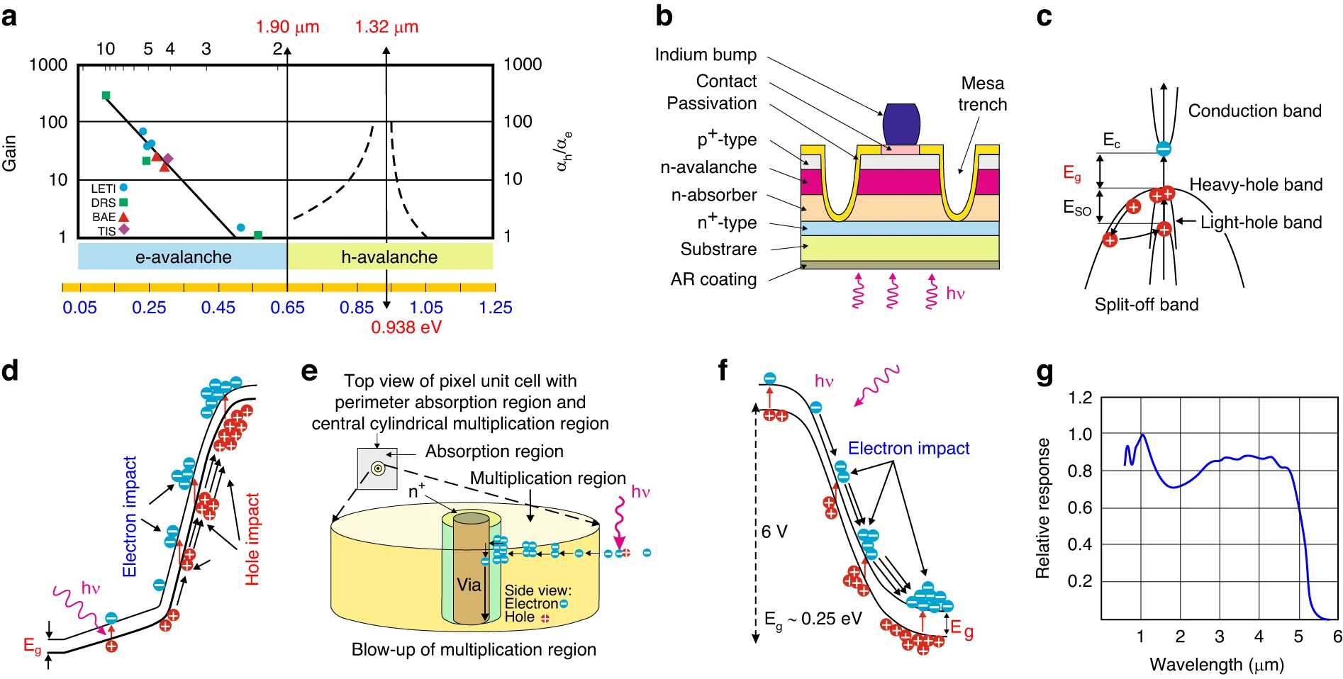
Fig. 6: Gain and k versus Hg1–xCdxTe bandgap energy. a the crossover between e-APD and h-APD. The crossover at Eg ≈ 0.65 eV corresponds to the λc = 1.9 μm for 300 K46. Hole-initiated avalanche HgCdTe photodiode: b detector profile, c energy band structure, d hole-initiated multiplication process energy band structure. The multiplication layer bandgap energy is adjusted to the resonance condition where the bandgap and the split-off valence band energy and the top of the heavy-hole valence band energy difference are equal. Electron-initiated avalanche HgCdTe photodiode: e diagram of electron-initiated avalanche process for HgCdTe-based high-density vertically integrated photodiode (HDVIP) structure (n-type central region and p-type material around), f electron avalanche mechanism, and g relative spectral response for 5.1 μm cut-off wavelength HgCdTe HDVIP at T = 80 K
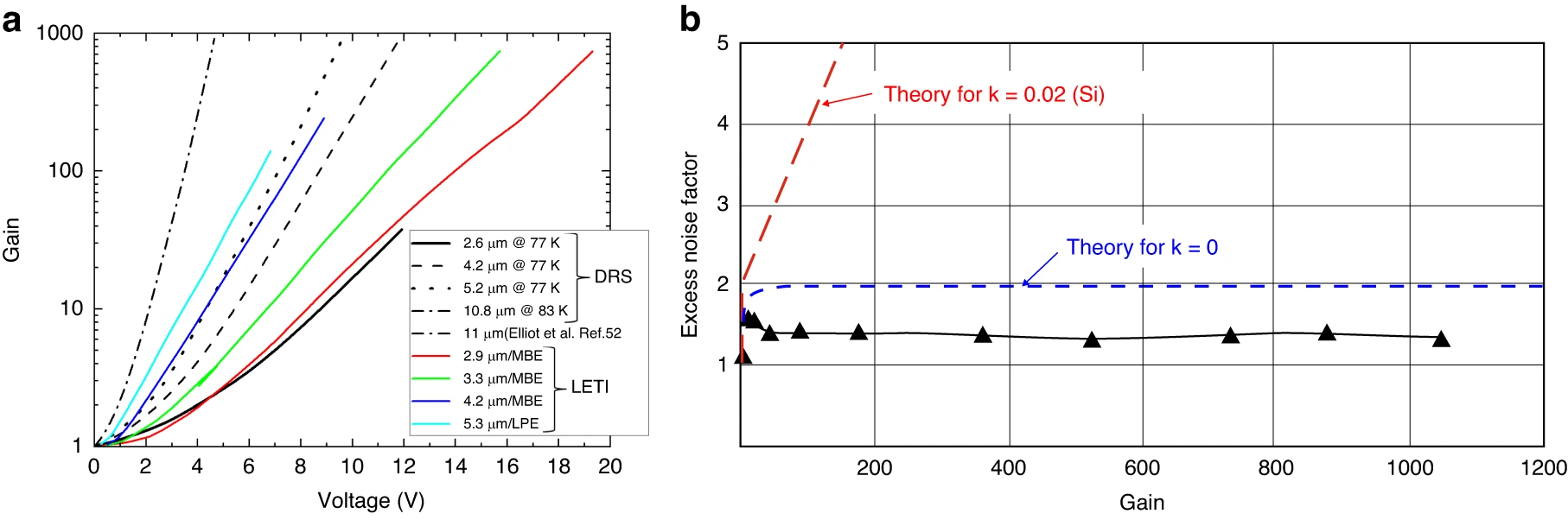
Fig. 7: HgCdTe APDs performance. a the experimental gain versus bias for selected cut-off wavelengths for DRS electron-initiated APDs at 77 K together with extra measured data points taken at ∼77 K51 and LETI e-APDs at 80 K59, b constant F(M) ~ 1 versus M at 80 K for 4.3 μm cut-off wavelength APD135
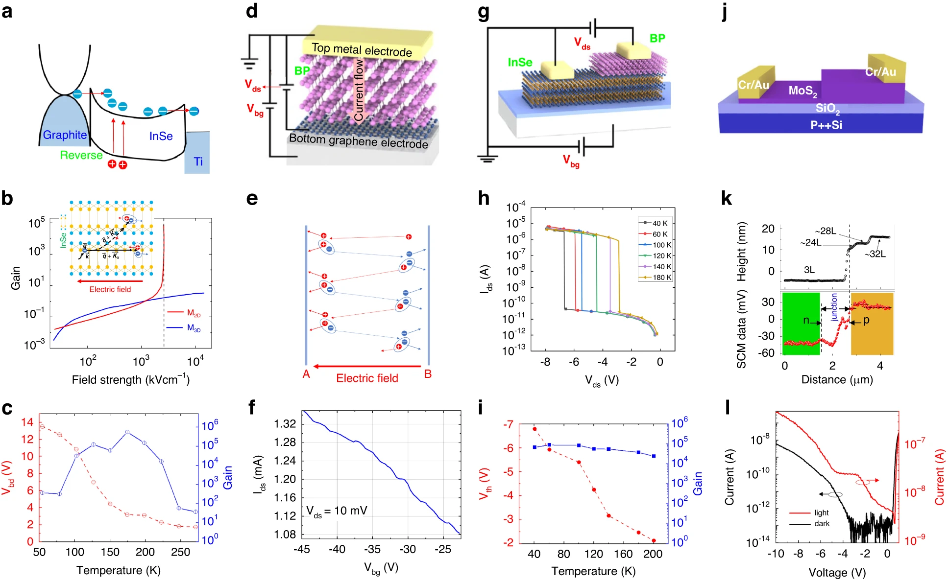
Fig. 9: Low-dimensional solid avalanche photodetectors. a graphite/InSe Schottky avalanche detector - injection, ionization, collection electron transport mechanisms, b e-ph scattering dimensionality reduction affects electron acceleration process and gain versus electric field in 2D (red line) and 3D (blue line), c breakdown voltage (Vbd) and gain as a function of temperature—exhibits a negative temperature coefficient81. Nanoscale vertical InSe/BP heterostructures ballistic avalanche photodetector: d schematic of the graphene/BP/metal avalanche device83, e ballistic avalanche photodetector operating principle, f quasi-periodic current oscillations, g schematic of the graphene InSe/BP83, h Ids–Vds characteristics for selected temperatures (40 − 180 K), i avalanche breakdown threshold voltage (Vth) and gain versus temperature—showing a negative temperature coefficient. Pristine PN junction avalanche photodetector: j device structure, k as the number of layers increases, a positive/negative signal of SCM denotes hole/electron carries, l APD’s low temperature (~100 K) dark and photocurrent I–V curves
excellent review paper
ReplyDelete