The first article in the Sensors special issue for IISW2023 is now available:
https://www.mdpi.com/1424-8220/23/18/7959
Chao et al. from TSMC in a paper titled "Random Telegraph Noise Degradation Caused by Hot Carrier Injection in a 0.8 μm-Pitch 8.3Mpixel Stacked CMOS Image Sensor" write:
In this work, the degradation of the random telegraph noise (RTN) and the threshold voltage (Vt) shift of an 8.3Mpixel stacked CMOS image sensor (CIS) under hot carrier injection (HCI) stress are investigated. We report for the first time the significant statistical differences between these two device aging phenomena. The Vt shift is relatively uniform among all the devices and gradually evolves over time. By contrast, the RTN degradation is evidently abrupt and random in nature and only happens to a small percentage of devices. The generation of new RTN traps by HCI during times of stress is demonstrated both statistically and on the individual device level. An improved method is developed to identify RTN devices with degenerate amplitude histograms.
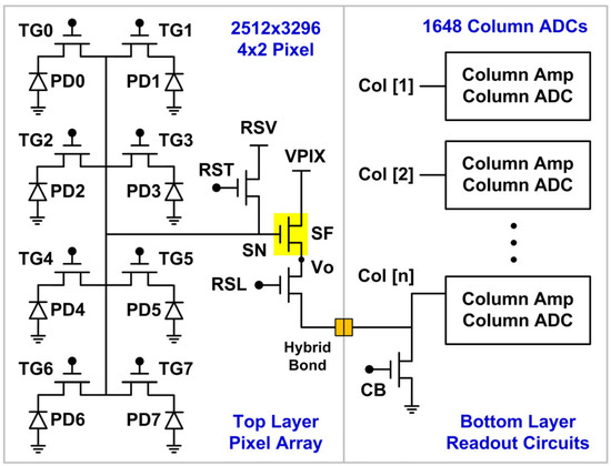
Figure 1. Simplified test chip architecture. The device under stress is the source follower (SF) NMOS in the 4 × 2-shared pixels on the top layer. The PD0–7 are the photodiodes, and the TG0–7 are the transfer gates in each 4 × 2-shared pixel. The total number of SF is 628 × 1648 = 1.03 M.
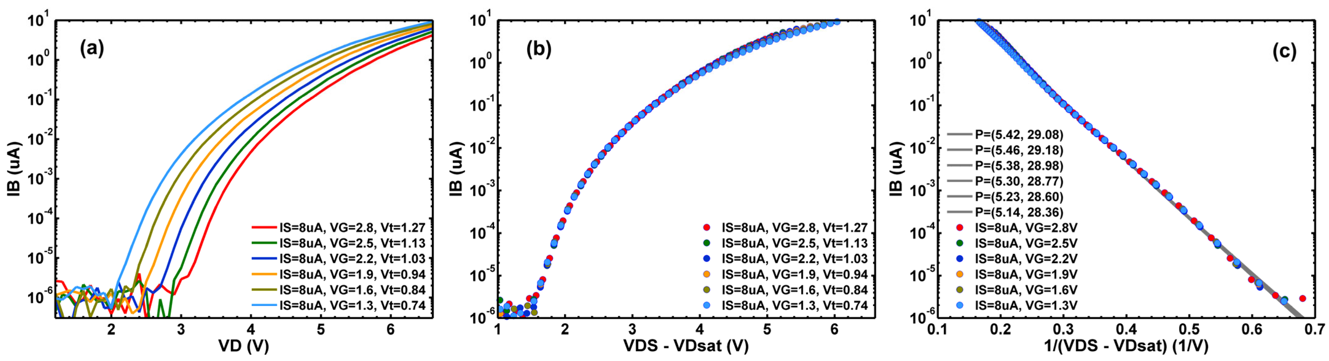
Figure 2. (a) The measured IB of a SF device vs. VD with VG stepping from 1.3 V to 2.8 V; (b) The same data as in (a) but plotted against VDS−VDsat≈VD−VG+Vt with Vt as a fitting parameter; (c) The same data as in (b) plotted against 1/(VDS−VDsat) with P=(P1,P2) as two fitting parameters according to Equation (1).
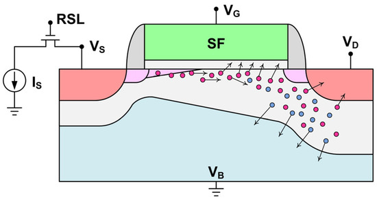
Figure 3. The bias configuration of the SF under test. The red and blue solid circles symbolize electrons and holes, respectively.
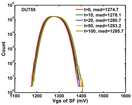
Figure 4. The histograms of the measured VGS of the SF for stress time (t) from 0 to 100 min.
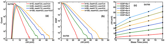
Figure 5. (a) The histograms of the threshold voltage shift (ΔVt) after 10-, 20-, 50-, and 100-min stress; (b) The inverse cumulative distribution function (ICDF) curves of ΔVt; (c) the constant ICDF contours against stress time (t).
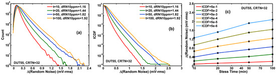
Figure 6. (a) The histograms of the random noise changes (ΔRN) after 10, 20, 50, 100 min stress; (b) The inverse cumulative distribution function (ICDF) curves; (c) the constant ICDF contours as functions of stress time (t).
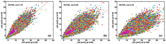
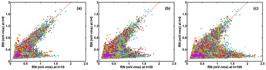
Figure 8. The correlation of the random noises (RN) before HCI stress (t = 0) vs. after (a) 10 min, (b) 20 min, and (c) 100 min stress, respectively The RN increases are noticeably nonuniform. The RN along the x = y red dash line remains relatively unchanged. The devices on the lower-right branches show a significant increase in RN. The population of the lower branch increases as stress time increases. Random colors are assigned to the data points to separate the dots from each other.
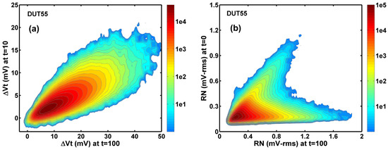
Figure 9. The 2D histograms of the correlation of the Vt shift and RN degradation shows dramatically different statistical behaviors. (a) The Vt change after 100-min stress versus that after 10-min stress. (b) The RN after 100 min stress versus that before the stress.
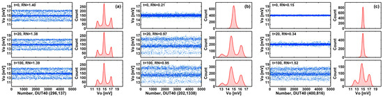
Figure 10. Generation of RTN traps during HCI stress. The 5000-frame waveforms before (t = 0) and after the HCI stress (t = 20, 100 min) with the corresponding histograms are shown for three selected examples. (a) Device (296, 137) shows one trap before stress and remains unchanged after stress. (b) Device (202, 1338) shows no trap before stress and one trap generated after 20 min of stress. (c) Device (400, 816) shows no trap before stress; however, one trap is generated after 100 min of stress. The RN unit is mV-rms.
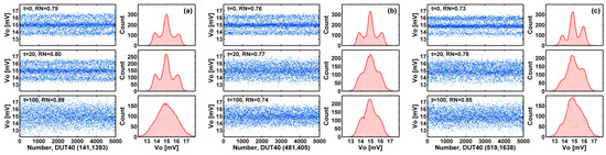
Figure 11. Degeneration of the RTN discrete levels. During HCI stress, the non-RTN noises may be increased significantly such that the discrete RTN levels become indistinguishable. (a) Device (141, 1393) show such degeneration after 100 min of stress. (b) Device (481, 405) show degeneration after 20 min of stress. (c) Device (519, 1638) shows unsymmetric side peaks and unsymmetric degeneration after 20 min and 100 min of stresses. The RN unit is mV-rms.
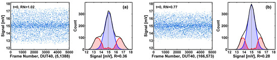
Figure 12. For devices showing a single histogram peak, if the histogram is significantly different from the Gaussian distribution, they are counted as RTN-like devices. The ratio R expressed in Equation (2) is defined as the red area versus the total area under the black histogram. The R values in examples (a) and (b) are 36% and 28%, respectively. The RN unit is mV-rms.
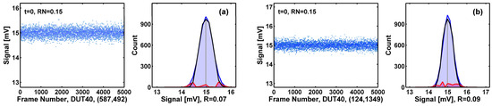
Figure 13. Devices with amplitude distributions close to Gaussian are considered as non-RTN devices. The deviation ratio R is 7% for device (587, 492) in (a) and 9% for device (124, 1349) in (b). The RN unit is mV-rms.
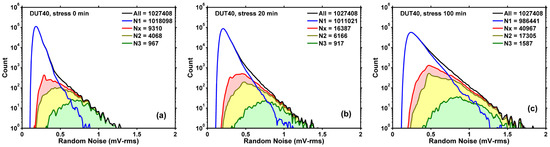
Figure 14. The RN distribution of the RTN and non-RTN devices, sorted by the improved algorithm: (a) before HCI stress, (b) after 20 min stress, and (c) after 100 min stress. The RTN devices clearly contribute to and dominate the long tails of the RN histograms. The number of RTN devices (Nx) (with the R-threshold set to 15%) increases systematically as the stress time increases.
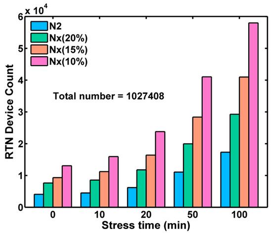
Figure 15. The count of RTN devices increases consistently as stress time increases. N2 is the number of devices showing two or more peaks in amplitude histograms. Nx is N2 plus the number of RTN-like devices determined by setting the R-threshold to 10%, 15%, and 20%, respectively.
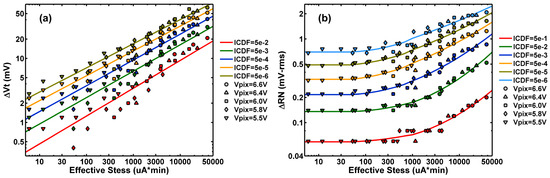
Figure 16. (a) The Vt shift and (b) the RN degradation trends against the effective stress defined in Equation (3), where the effectiveness factors are treated as empirical fitting parameters such that all the constant-ICDF points for different voltages fall onto a family of continuous and smooth curves. The fitting results are listed in Table 1.
No comments:
Post a Comment
All comments are moderated to avoid spam and personal attacks.