Kim et al. from imec and coauthors from universities in Belgium and Korea recently published a paper titled "A Thin-Film Pinned-Photodiode Imager Pixel with Fully Monolithic Fabrication and beyond 1Me- Full Well Capacity" in MDPI Sensors. This paper describes imec's recent thin film pinned photodiode technology.
Open access paper link: https://www.mdpi.com/1424-8220/23/21/8803
Abstract
Thin-film photodiodes (TFPD) monolithically integrated on the Si Read-Out Integrated Circuitry (ROIC) are promising imaging platforms when beyond-silicon optoelectronic properties are required. Although TFPD device performance has improved significantly, the pixel development has been limited in terms of noise characteristics compared to the Si-based image sensors. Here, a thin-film-based pinned photodiode (TF-PPD) structure is presented, showing reduced kTC noise and dark current, accompanied with a high conversion gain (CG). Indium-gallium-zinc oxide (IGZO) thin-film transistors and quantum dot photodiodes are integrated sequentially on the Si ROIC in a fully monolithic scheme with the introduction of photogate (PG) to achieve PPD operation. This PG brings not only a low noise performance, but also a high full well capacity (FWC) coming from the large capacitance of its metal-oxide-semiconductor (MOS). Hence, the FWC of the pixel is boosted up to 1.37 Me- with a 5 μm pixel pitch, which is 8.3 times larger than the FWC that the TFPD junction capacitor can store. This large FWC, along with the inherent low noise characteristics of the TF-PPD, leads to the three-digit dynamic range (DR) of 100.2 dB. Unlike a Si-based PG pixel, dark current contribution from the depleted semiconductor interfaces is limited, thanks to the wide energy band gap of the IGZO channel material used in this work. We expect that this novel 4 T pixel architecture can accelerate the deployment of monolithic TFPD imaging technology, as it has worked for CMOS Image sensors (CIS).
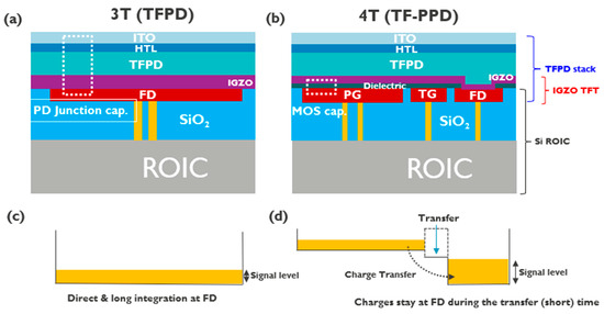
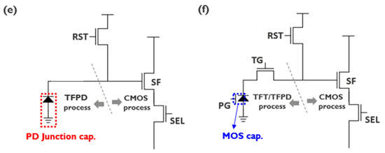
Figure 1. Pixel cross-section for the monolithic TFPD image sensor (a) 3 T and (b) 4 T (TF-PPD) structure (TCO: transparent conductive oxide, HTL: hole transport layer, PG: photogate, TG: transfer gate, FD: floating diffusion). Electric potential and signal readout configuration for 3 T pixel (c) and for 4 T pixel (d). Pixel circuit diagram for 3 T pixel (e) and for the 4 T pixel (f).
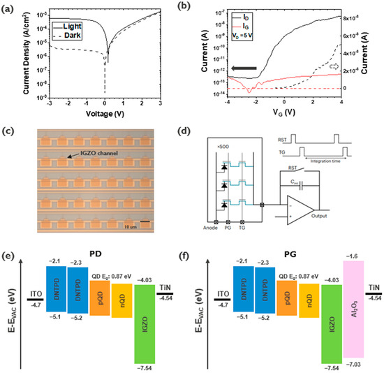
Figure 2. I-V characteristic of QDPD test structure (a) and of IGZO TFT (b), a micrograph of the TF-PPD passive pixel array (c), and its measurement schematic (d). Band diagrams for the PD (e) and PG (f).
Figure 3. Silvaco TCAD simulation results; (a) simulated structure, (b) lateral potential profile along the IGZO layer, and (c) potential profile when TG is turned off and (d) on.
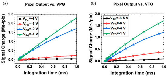
Figure 4. Signal output vs. integration time with different VPG and VTG values with the illumination. Signal curves with the fixed VTG (−1 V), varying VPG (−4~−1 V) (a), the same graphs for the fixed VPG (−2 V), and different VTGs (−6.5~−1 V) (b).
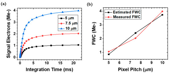
Figure 4. Signal output vs. integration time with different VPG and VTG values with the illumination. Signal curves with the fixed VTG (−1 V), varying VPG (−4~−1 V) (a), the same graphs for the fixed VPG (−2 V), and different VTGs (−6.5~−1 V) (b).
Figure 5. (a) Pixel output vs. integration time for different pixel pitches. (b) FWC comparison between estimation and measurement.
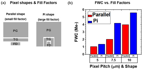
Figure 6. FWC comparison by different pixel fill factors. Pixel schematics for different shapes (a), and FWC by different pixel shapes and pitches (b).

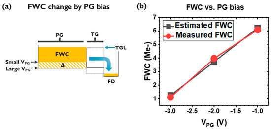
Figure 7. Potential diagram describing FWC increase by the larger VPG (a), and FWC vs. VPG (b).
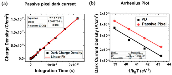
Figure 8. Passive pixel dark current (a) and Arrhenius plots (b) for the QDPD test structure and the passive pixel.
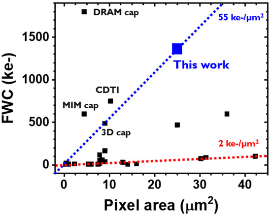
Figure 9. FWC vs. pixel area. A guideline showing the FWC density per unit area for this work (blue) and a trend line for the most of CISs (red).
No comments:
Post a Comment
All comments are moderated to avoid spam and personal attacks.