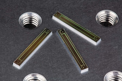
Emberion, Graphenea, and AMO have been approved a European Innovation Council Fast Track to Innovation (FTI) project to help bring to the market the G-IMAGER, a graphene imager based on graphene-on-wafer technology. The G-Imager is a SWIR detector for applications in semiconductor inspection, sorting systems, spectroscopy hyperspectral imaging and surveillance. The projected market size for SWIR cameras in 2020 is around $1 billion.
The G-Imager will be based on the scientifically proven operation of a graphene channel coupled to nanocrystal light absorbers. The nanocrystals serve the function of strong light absorbers for high efficiency, whereas the graphene channel efficiently transports the generated charge to electrical contacts for detection. The benefits of G-Imager compared to other SWIR detectors, apart from the dramatic cost reduction, will be a lack of cooling requirements, low noise, large dynamic range, broad spectral range and scalable pixel size. These benefits guarantee quick market uptake of the product beyond the project duration, which is 24 months.
To bring G-Imager to the market, the project consortium will have to tackle challenges related to maturing the innovation. Namely, the production process yield for the detectors meeting a specified set of quality requirements must be guaranteed at a minimum of 85%, which is an industry standard. The technology readiness level must be raised to level 8, while scaling up the production process to meet volume requirements. Graphenea will scale up production of 200mm graphene-on-wafers to 10,000 wafers/year. A key project goal is integration into semiconductor production processes, such that G-Imager production is compatible with demanding requirements of the foundries where high-volume semiconductor device production takes place, like the foundry at AMO GmbH. AMO will develop a new “graphene device foundry service” to industrialize production of the photodetector. The SWIR detector production will be finalized at Emberion, where VGA resolution imager products will be made by depositing and patterning photosensitive materials on the graphene devices. Product finalization includes encapsulation, dicing and packaging the final imager products and integrating them into Emberion’s camera core products.
The consortium expects the project to assist in raising the cumulative net income of the consortium members to 60M€ in 4 years.
In a separate announcement, Emberion is to present a cost-competitive 512× 1 pixel VIS-SWIR linear array sensor for visible light to shortwave infrared (VIS-SWIR) detection at SPIE Photonics West in San Francisco on February 5-7, 2019. The sensor provides superior and consistent responsivity with very low noise over the broad (400 – 1800 nm) spectral range. The sensor is primarily designed for spectrometry applications. The sensor comprises an array of 25 × 500 µm2 pixels monolithically built on a tailor-made CMOS ROIC.
Beyond the linear array product introduced, Emberion will offer VGA imagers in late 2019. These VGA sensors cover the same VIS-SWIR spectral range (400-1800 nm wavelength) and are well suited for night and machine vision as well as hyperspectral imaging.
A 2017 Nature paper explains how the company's graphene imagers work:


Well... how to say... « too good to be true » maybe?
ReplyDeletethere are many swir applications in semiconductor assembly environment that dont get realized because ingaas is very expensive even at low resolutions. A product offering price drop and resolution increase to image in the 1500nm range would get quite some demand...
ReplyDeleteIf I do the math on the plot shown on the first picture, I get 0.0023 A/W @ 910 nm, which is a poor sensitivity. Maybe the fill factor of the sample was low??? Any silicon device can do better...
ReplyDeleteMay be they've managed to improve this since 2017 when this paper was written? The new improvement they claim now is:
Delete"scientifically proven operation of a graphene channel coupled to nanocrystal light absorbers. The nanocrystals serve the function of strong light absorbers for high efficiency, whereas the graphene channel efficiently transports the generated charge to electrical contacts for detection."
When I first read this, I was thinking that I had no idea what this really meant. Still true. Is it still based on piezoelectric nanocrystals? Is the charge generated by temperature change in the piezoelectric nanocrystal? What is special about graphene for transporting charge? Metals and semiconductors work pretty well most of the time for transporting charge. Maybe the funding magic is in the use of graphene? I recall from the 80's that a big drawback with piezoelectrics for IR detection is their sensitivity of microphonics and temperature bias sensitivity.
DeleteI have no idea either. If these were piezoelectric nanocrystals, they would be able to sense much wider spectral band than SWIR. So, I'd guess this is something different.
DeleteWhen I read the announcement, my best guess was a colloidal quantum dot such as PbS, which has a band gap that is tunable into the short-wave infrared. A few research groups have demonstrated that a 2D material channel coupled to a quantum dot absorber can lead to enhanced short-wave infrared sensing. https://pubs.acs.org/doi/abs/10.1021/acsphotonics.9b00870
DeleteWhen we started the 2wideSense project, we have envisionned a VGA InGaAs sensor for automobile use at less than 50$ unit ... Many years passed, it is still a dream.
ReplyDeletehttp://image-sensors-world.blogspot.com/2013/08/2widesense-final-report.html
Could you tell more about that project and why it was unsuccessful? The URLs in the text you linked are not active any more.
DeleteI'd like to see a reference to the claim of a $1B market in 2020. That's totally ridiculous. Such wildly exaggerated projections really goes to the credibility of the author and anyone who's research comes up with such a number.
ReplyDeleteAgree!
DeleteGuess graphene and nanocrystal interface shows much lower defect density therefore less dark current generation, or maybe band alignment in between can facilitate charge transfer as there is no schottky barrier caused by pinning.
ReplyDelete