Eric Fossum, Nobukazu Teranishi, and Albert Theuwissen have published a review paper titled "Digital Image Sensor Evolution and New Frontiers" in the Annual Review of Vision Science.
Link: https://doi.org/10.1146/annurev-vision-101322-105538
Abstract:
This article reviews nearly 60 years of solid-state image sensor evolution and identifies potential new frontiers in the field. From early work in the 1960s, through the development of charge-coupled device image sensors, to the complementary metal oxide semiconductor image sensors now ubiquitous in our lives, we discuss highlights in the evolutionary chain. New frontiers, such as 3D stacked technology, photon-counting technology, and others, are briefly discussed.
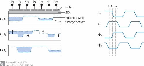
Figure 1 Illustration of a four-phase charge-coupled device diagram, a potential well diagram, and clock charts. As four clocks switch sequentially, the potential wells move rightward together with the charge packets.
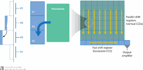
Figure 2 Illustration of a (three-phase) interline-transfer (ILT) charge-coupled device (CCD) showing (left) a unit cell with a photodiode (PD) and vertical CCD and (right) the entire ILT CCD image sensor. The photosignal moves from the PD into the vertical CCD, and then into the horizontal CCD to the sense node and output amplifier.
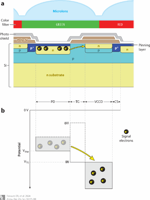
Figure 3 A pinned PD in an interline-transfer CCD with one phase of the CCD shift register (VCCD) shown. (a) A physical cross-section and (b) a potential diagram showing the electrons transferring from the PD to the VCCD. Abbreviations: CCD, charge-coupled device; CS, channel stop; PD, photodiode; TG, transfer gate; VCCD, vertical CCD.
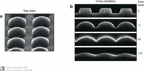
Figure 4 Microlenses to concentrate light on the photoactive area of a pixel. (a) Top view. (b) Cross-sections for different thermal-flow times. Images courtesy of NEC Corp.

Figure 5 A 16-Mpixel stitched complementary metal oxide semiconductor image sensor on a 6-inch-diameter wafer. Figure reproduced from Ay & Fossum (2006).
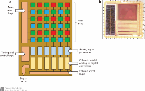
Figure 6 (a) Complementary metal oxide semiconductor (CMOS) image sensor block diagram. (b) Photograph of early Photobit CMOS image sensor chip for webcams. (Left) Digital logic for control and input-output (I/O) functions. (Top right) The pixel array. (Bottom right) The column-parallel analog signal processing and analog-to-digital converter (ADC) circuits. Photo courtesy of E.R.F.

Figure 7 An illustrative PPD 4-T active pixel with intrapixel charge transfer. (a) A circuit schematic (Fossum & Hondongwa 2014). (b) A band diagram looking vertically through the PPD showing the photon, electron–hole pair, and SW. (c) A physical cross-section showing doping levels (Fossum 2023). Abbreviations: COL BUS, column bus line; FD, floating diffusion; PPD, pinned photodiode; RST, reset gate; SEL, select gate; SF, source-follower; SW, storage well; TG, transfer gate.
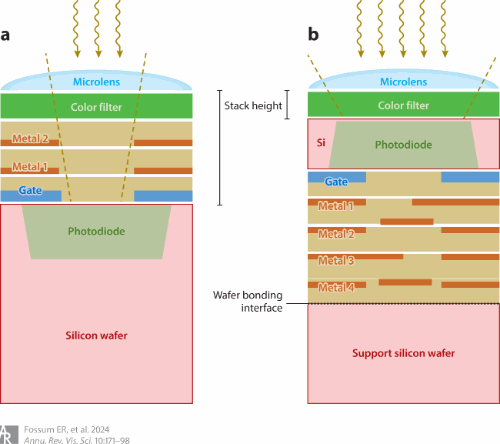
Figure 8 Illustrative example of (a) a frontside-illuminated pixel and (b) a backside-illuminated (BSI) pixel showing the better light gathering capability of the BSI pixel.
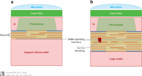
Figure 9 Illustrative cross-sectional comparison of (a) a backside-illuminated device and (b) 3D stacked image sensors where the lower layer is used for additional circuitry.
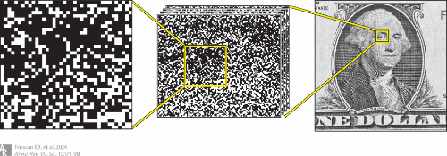
Figure 10 Quanta image sensor concept showing the spatial distribution of jot outputs (left), an expanded view of jot output bit planes at different time slices (center), and gray-scale image pixels formed from spatiotemporal neighborhoods of jots (right). Figure adapted from Ma et al. (2022a).
This invited paper took us a long time to prepare! It is the first paper the 3 of us have written together and I'm glad for that.
ReplyDeleteThis paper is so useful for teaching our students the foundations of CIS, thank you for posting this. The illustrations are beautiful!
ReplyDelete