In a paper titled "" Eom et al. from Yonsei University, EPFL, Sungkyunkwan University and TruPixel, Inc. write:
This paper presents a process-controlled study of illumination engineering in single-photon avalanche diodes (SPADs) fabricated in a 110 nm standard CMOS image sensor (CIS) technology. Front-illuminated (FI) and back-illuminated (BI) SPADs were implemented with identical front-end-of-line (FEOL) structures, including the junction and guard-ring configurations, enabling the isolation of the effects of illumination direction and back-end-of-line (BEOL) configuration without modifying the junction structure. Through TCAD simulations and comprehensive experimental characterizations, including current–voltage, light-emission, dark count rate (DCR), photon detection probability (PDP), and timing-jitter measurements, we systematically analyze the performance trade-offs introduced by the BI configuration. The BI SPAD exhibits enhanced near-infrared PDP and a broader spectral response due to its deeper absorption region and the incorporation of a metal reflector, while maintaining identical avalanche characteristics, as evidenced by an unchanged 72 ps full-width-at-half-maximum (FWHM) timing jitter. However, the backside illumination increases the diffusion tail, indicating a trade-off between near-infrared sensitivity and diffusion-related timing performance. These results provide design guidelines for optimizing SPAD performance through illumination-direction and BEOL engineering while preserving the FEOL design and demonstrate a useful approach for SPAD integration in standard CMOS technology.
Link: https://www.mdpi.com/1424-8220/26/5/1664
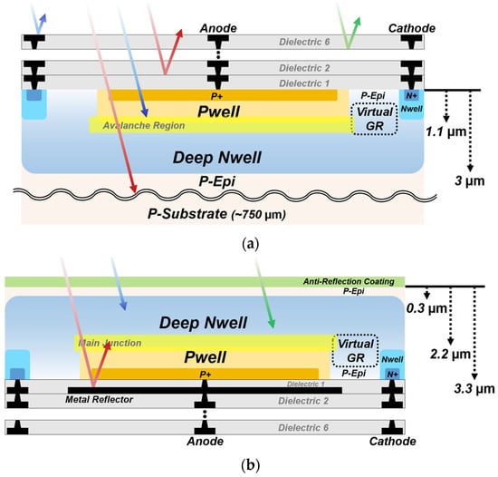
Figure 1. Cross-sections of the SPADs with different illumination configurations: (a) FI SPAD; (b) BI SPAD.
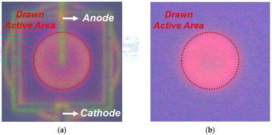
Figure 5. LET results of the SPADs at Vex = 3 V, visualizing avalanche emission across the active area: (a) FI SPAD; (b) BI SPAD.
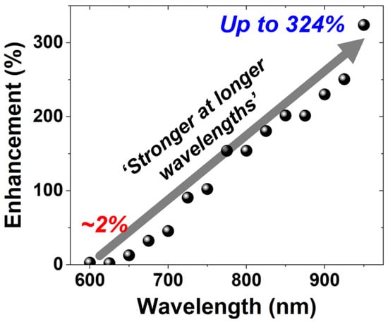
Figure 10. Wavelength-dependent PDP enhancement of the BI SPAD over the FI SPAD.

No comments:
Post a Comment
All comments are moderated to avoid spam and personal attacks.