ON Semi shows a demo of its Pandion sensor, a 400 x 100 SPAD array sensor for LiDAR applications:
Wednesday, April 22, 2020
Tuesday, April 21, 2020
Intel Capital Imaging Portfolio: Trieye SWIR, Prophesee Event-Based Sensor
Avi Bakal, Trieye CEO & Co-Founder, talks about SWIR imaging in automotive applications:
Luca Verre, Prophesee CEO & Co-Founder, talks about event driven vision:
Luca Verre, Prophesee CEO & Co-Founder, talks about event driven vision:
Espros Reviews Ways to Failsafe ToF Imager
Espros April Newsletter discusses the ways to failsafe a ToF Camera:
Time-of-flight cameras are often used in safety crirical applications, e.g. in anti-collision sensors for robots. It's evident, that the sensor is working correctly or, in case of a malfunction, the control system of the of the robot detects a malfunction. A serious fault in a TOF camera is the failure of one or more pixels of the TOF imager. Whereas a «stuck--at» failure is relatively easy to detect, a floating signal which can randomly take any state is not.
A pixel in an imager can be faulty in a way that it reports any level in grayscale from fully dark to fully bright. This can also be the case in a TOF imager. Thus, in a safety critical application, the distance to an object reported by a pixel is assumed to be wrong. The pixel can report the correct distance within a given tolerance band or any other distance which is not correct. Such behavior is fatal in an anti-collision sensor based on a 3D camera. The question now is, how to detect incorrect distance reporting pixels.
There are several ways to do so:
Time-of-flight cameras are often used in safety crirical applications, e.g. in anti-collision sensors for robots. It's evident, that the sensor is working correctly or, in case of a malfunction, the control system of the of the robot detects a malfunction. A serious fault in a TOF camera is the failure of one or more pixels of the TOF imager. Whereas a «stuck--at» failure is relatively easy to detect, a floating signal which can randomly take any state is not.
A pixel in an imager can be faulty in a way that it reports any level in grayscale from fully dark to fully bright. This can also be the case in a TOF imager. Thus, in a safety critical application, the distance to an object reported by a pixel is assumed to be wrong. The pixel can report the correct distance within a given tolerance band or any other distance which is not correct. Such behavior is fatal in an anti-collision sensor based on a 3D camera. The question now is, how to detect incorrect distance reporting pixels.
There are several ways to do so:
- Comparison: Comparison of the reported distance with a known distance (comparison). This can be applied e.g. in a door sensor where the sensor looks from top of the door down to the floor.
- Offset: Adding a delay into the illumination path (or the demodulation path) to impose a virtual distance shift. By subtracting the distance shift imposed by the delay, the same or a similar distance as the one without delay should be resulting.
- Scaling: Changing the modulation frequency but not changing the distance calculation parameters accordingly. This is similar like 3., but the distance shift is not fix, it is dependent on the distance value.
- Pattern: By changing the modulation or demodulation pattern, good pixels report the same (correct) distance even in a different phase sequence.
- Fill & Spill: Inject a defined amount of charge into a pixel and check the response of the pixel.
Heliotis White Light Interferometric 3D Sensor
Heliotis releases more info about its Series 4 while light interferometric 3D sensor:
"It’s basis is a CMOS 2D array in which each individual pixel picks up and processes the optical signal in parallel. In this SmartPixel concept each pixel has an electronic circuit for real-time image processing.
The light reflected by the sample is combined with a reference signal. This results in an interferometric signal from which the desired depth information can be derived mathematically. The system works non-invasively and non-contact in a wide range of objects and materials with a spatial resolution of microns.
The new generation of WLI sensors has been developed from scratch. We put in over 10 years of experience from Series 1, 2 and 3."

Thanks to TL for the info!
"It’s basis is a CMOS 2D array in which each individual pixel picks up and processes the optical signal in parallel. In this SmartPixel concept each pixel has an electronic circuit for real-time image processing.
The light reflected by the sample is combined with a reference signal. This results in an interferometric signal from which the desired depth information can be derived mathematically. The system works non-invasively and non-contact in a wide range of objects and materials with a spatial resolution of microns.
The new generation of WLI sensors has been developed from scratch. We put in over 10 years of experience from Series 1, 2 and 3."

Thanks to TL for the info!
Samsung is Aiming for 600MP Sensor, IR, UV, Multispectral
Samsung publishes an article "Rivaling the Human Eye: How Samsung is Opening Up the Possibilities for Image Sensor Technology" by Yongin Park, EVP, Head of Sensor Business Team, System LSI Business. Few quotes:
"The image sensors we ourselves perceive the world through – our eyes – are said to match a resolution of around 500 megapixels (Mp). Compared to most DSLR cameras today that offer 40Mp resolution and flagship smartphones with 12Mp, we as an industry still have a long way to go to be able to match human perception capabilities.
Aiming for 600Mp for All
To date, the major applications for image sensors have been in the smartphones field, but this is expected to expand soon into other rapidly-emerging fields such as autonomous vehicles, IoT and drones. Samsung is proud to have been leading the small-pixel, high-resolution sensor trend that will continue through 2020 and beyond, and is prepared to ride the next wave of technological innovation with a comprehensive product portfolio that addresses the diverse needs of device manufacturers.
Through relentless innovation, we are determined to open up endless possibilities in pixel technologies that might even deliver image sensors that can capture more detail than the human eye."

"The image sensors we ourselves perceive the world through – our eyes – are said to match a resolution of around 500 megapixels (Mp). Compared to most DSLR cameras today that offer 40Mp resolution and flagship smartphones with 12Mp, we as an industry still have a long way to go to be able to match human perception capabilities.
Aiming for 600Mp for All
To date, the major applications for image sensors have been in the smartphones field, but this is expected to expand soon into other rapidly-emerging fields such as autonomous vehicles, IoT and drones. Samsung is proud to have been leading the small-pixel, high-resolution sensor trend that will continue through 2020 and beyond, and is prepared to ride the next wave of technological innovation with a comprehensive product portfolio that addresses the diverse needs of device manufacturers.
Through relentless innovation, we are determined to open up endless possibilities in pixel technologies that might even deliver image sensors that can capture more detail than the human eye."

Caeleste Proposes "True Charge Domain Binning"
Caeleste patents a true charge domain binning method by making a number of pixels “non-collecting”. The photo charge that is not collected by these pixels is then collected by drift or diffusion by the other pixels in the kernel.
While other companies might call it blooming, Caeleste implements pixel binning in that same way:


While other companies might call it blooming, Caeleste implements pixel binning in that same way:


Monday, April 20, 2020
Article on Pixel Scaling: DTI, High-k, 0.6um Pitch, More
Semiconductor Engineering site publishes an article "Scaling CMOS Image Sensors" by Mark Lapedus. Few quotes:
Recently, vendors have ironed out the issues and the pixel scaling race has resumed. In 2018, Samsung broke the 1µm barrier with 0.9µm, followed by Sony with 0.8µm in 2019, and Samsung with 0.7µm in 2020.
For sub-µm pixel scaling, the industry requires more innovations. “As pixels shrink, thicker active (silicon) is required to maintain a suitable photodiode size,” [TechInsights analyst Ray] Fontaine said in a recent presentation. “A key technology enabler for thicker active (silicon) is DTI and associated high-k defect passivation films.”
Making an image sensor with high-k films follows a traditional flow. What’s different is that high-k films are deposited over the liner in the DTI trenches.
For high-k and other processes, vendors take two different approaches in the fab—front-DTI (F-DTI) and back-DTI (B-DTI). “F-DTI uses a poly silicon gap fill, and the poly can have voltage bias for improved surface pinning. F-DTI can also have more thermal treatment for etch damage leakage reduction,” OmniVision’s [SVP of Process Engineering Lindsay] Grant said. “B-DTI uses high-k films with a negative charge to accumulate charge and pin the Fermi level at the surface, which then suppresses dark-current leakage. The high-k film process is atomic layer deposition (ALD). B-DTI typically uses an oxide gap fill, but some metal fill and even air gap have also been tried and used in mass production.”
Will pixel scaling continue? “It’s likely that pixel scaling will continue beyond 0.7µm,” Grant said. “As pixels shrink beyond 0.7µm, many aspects need to be optimized. Key items, such as B-DTI, high-energy implant for deep diode, optical structure shrink for color and microlens, will remain the focus for development. The more basic design rules that define in-pixel transistors and interconnects need to be updated.”
Another issue is that the pixel pitch for mobile sensors is approaching the wavelength of light. “Some people may consider this a limit for minimum pixel size,” Grant said. “For example, the 0.6µm pixel pitch is used in R&D today. This is smaller than the wavelength of red light at 0.65µm (650nm). So the question may arise, ‘Why shrink to sub-wavelength? Will there be any useful benefit for the camera user? Shrinking the pixel size to sub-wavelength does not mean there is no valuable spatial resolution information at the pixel level.’”
Grant pointed out that the optical structures for a 1.0µm pixel use many sub-wavelength features. “For example, narrow metal grids for crosstalk suppression and narrow dielectric walls for quantum-efficiency are seeing improvement through light guiding. This nano-scale optical engineering is already in current pixels and has been for many years, so moving to sub-wavelength is not such a revolution,” he said. “The limitation for continued shrink may come from the user benefit rather than the technology. Today, applications continue to find end user value in shrinking the pixel size, so this is driving the trend. As long as that continues, CMOS image sensor technology development will support that direction.”
The next big thing is pixel-to-pixel interconnects. Xperi is developing a technology called “3D Hybrid BSI” for pixel-level integration. Sony and OmniVision have demonstrated the technology.
“It enables more interconnects,” said Abul Nuruzzaman, senior director of product marketing at Xperi. “It allows pixel-level interconnect between each pixel of the sensor and an associated A/D converter. This allows parallel A/D conversion for all pixels. The connection provides high-density electrical interconnection between the stacked pixel and logic layers, allowing implementation of as many A/D converters as the number of effective megapixels. Hybrid bonding can also be used to stack memory with dedicated memory to each pixel.”
Recently, vendors have ironed out the issues and the pixel scaling race has resumed. In 2018, Samsung broke the 1µm barrier with 0.9µm, followed by Sony with 0.8µm in 2019, and Samsung with 0.7µm in 2020.
For sub-µm pixel scaling, the industry requires more innovations. “As pixels shrink, thicker active (silicon) is required to maintain a suitable photodiode size,” [TechInsights analyst Ray] Fontaine said in a recent presentation. “A key technology enabler for thicker active (silicon) is DTI and associated high-k defect passivation films.”
Making an image sensor with high-k films follows a traditional flow. What’s different is that high-k films are deposited over the liner in the DTI trenches.
For high-k and other processes, vendors take two different approaches in the fab—front-DTI (F-DTI) and back-DTI (B-DTI). “F-DTI uses a poly silicon gap fill, and the poly can have voltage bias for improved surface pinning. F-DTI can also have more thermal treatment for etch damage leakage reduction,” OmniVision’s [SVP of Process Engineering Lindsay] Grant said. “B-DTI uses high-k films with a negative charge to accumulate charge and pin the Fermi level at the surface, which then suppresses dark-current leakage. The high-k film process is atomic layer deposition (ALD). B-DTI typically uses an oxide gap fill, but some metal fill and even air gap have also been tried and used in mass production.”
Will pixel scaling continue? “It’s likely that pixel scaling will continue beyond 0.7µm,” Grant said. “As pixels shrink beyond 0.7µm, many aspects need to be optimized. Key items, such as B-DTI, high-energy implant for deep diode, optical structure shrink for color and microlens, will remain the focus for development. The more basic design rules that define in-pixel transistors and interconnects need to be updated.”
Another issue is that the pixel pitch for mobile sensors is approaching the wavelength of light. “Some people may consider this a limit for minimum pixel size,” Grant said. “For example, the 0.6µm pixel pitch is used in R&D today. This is smaller than the wavelength of red light at 0.65µm (650nm). So the question may arise, ‘Why shrink to sub-wavelength? Will there be any useful benefit for the camera user? Shrinking the pixel size to sub-wavelength does not mean there is no valuable spatial resolution information at the pixel level.’”
Grant pointed out that the optical structures for a 1.0µm pixel use many sub-wavelength features. “For example, narrow metal grids for crosstalk suppression and narrow dielectric walls for quantum-efficiency are seeing improvement through light guiding. This nano-scale optical engineering is already in current pixels and has been for many years, so moving to sub-wavelength is not such a revolution,” he said. “The limitation for continued shrink may come from the user benefit rather than the technology. Today, applications continue to find end user value in shrinking the pixel size, so this is driving the trend. As long as that continues, CMOS image sensor technology development will support that direction.”
The next big thing is pixel-to-pixel interconnects. Xperi is developing a technology called “3D Hybrid BSI” for pixel-level integration. Sony and OmniVision have demonstrated the technology.
“It enables more interconnects,” said Abul Nuruzzaman, senior director of product marketing at Xperi. “It allows pixel-level interconnect between each pixel of the sensor and an associated A/D converter. This allows parallel A/D conversion for all pixels. The connection provides high-density electrical interconnection between the stacked pixel and logic layers, allowing implementation of as many A/D converters as the number of effective megapixels. Hybrid bonding can also be used to stack memory with dedicated memory to each pixel.”
Fourier Ptychography Introduction
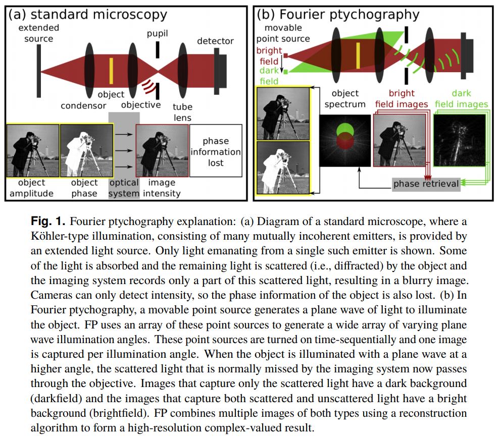
Duke University (USA), Advanced Research Center for Nanolithography (The Netherlands), Vrije Universiteit (The Netherlands), and University of Glasgow (UK) publish OSA Optics Express paper "Fourier ptychography: current applications and future promises" by Pavan Chandra Konda, Lars Loetgering, Kevin C. Zhou, Shiqi Xu, Andrew R. Harvey, and Roarke Horstmeyer.
"Traditional imaging systems exhibit a well-known trade-off between the resolution and the field of view of their captured images. Typical cameras and microscopes can either “zoom in” and image at high-resolution, or they can “zoom out” to see a larger area at lower resolution, but can rarely achieve both effects simultaneously. In this review, we present details about a relatively new procedure termed Fourier ptychography (FP), which addresses the above trade-off to produce gigapixel-scale images without requiring any moving parts. To accomplish this, FP captures multiple low-resolution, large field-of-view images and computationally combines them in the Fourier domain into a high-resolution, large field-of-view result. Here, we present details about the various implementations of FP and highlight its demonstrated advantages to date, such as aberration recovery, phase imaging, and 3D tomographic reconstruction, to name a few. After providing some basics about FP, we list important details for successful experimental implementation, discuss its relationship with other computational imaging techniques, and point to the latest advances in the field while highlighting persisting challenges."


"Traditional imaging systems exhibit a well-known trade-off between the resolution and the field of view of their captured images. Typical cameras and microscopes can either “zoom in” and image at high-resolution, or they can “zoom out” to see a larger area at lower resolution, but can rarely achieve both effects simultaneously. In this review, we present details about a relatively new procedure termed Fourier ptychography (FP), which addresses the above trade-off to produce gigapixel-scale images without requiring any moving parts. To accomplish this, FP captures multiple low-resolution, large field-of-view images and computationally combines them in the Fourier domain into a high-resolution, large field-of-view result. Here, we present details about the various implementations of FP and highlight its demonstrated advantages to date, such as aberration recovery, phase imaging, and 3D tomographic reconstruction, to name a few. After providing some basics about FP, we list important details for successful experimental implementation, discuss its relationship with other computational imaging techniques, and point to the latest advances in the field while highlighting persisting challenges."


Sunday, April 19, 2020
Multispectral Sensor with Hybrid Plasmonic CFA
University of Melbourne and Australian National Fabrication Facility publish AIP paper "A single sensor based multispectral imaging camera using a narrow spectral band color mosaic integrated on the monochrome CMOS image sensor" by Xin He, Yajing Liu, Kumar Ganesan, Arman Ahnood, Paul Beckett, Fatima Eftekhari, Dan Smith, Md Hemayet Uddin, Efstratios Skafidas, Ampalavanapillai Nirmalathas, and Ranjith Rajasekharan Unnithan.
"We demonstrate a single sensor based three band multispectral camera using a narrow spectral band red–green–blue color mosaic in a Bayer pattern integrated on a monochrome CMOS sensor. The narrow band color mosaic is made of a hybrid combination of plasmonic color filters and a heterostructured dielectric multilayer. The demonstrated camera technology has reduced cost, weight, size, and power by almost n times (where n is the number of bands) compared to a conventional multispectral camera."


"We demonstrate a single sensor based three band multispectral camera using a narrow spectral band red–green–blue color mosaic in a Bayer pattern integrated on a monochrome CMOS sensor. The narrow band color mosaic is made of a hybrid combination of plasmonic color filters and a heterostructured dielectric multilayer. The demonstrated camera technology has reduced cost, weight, size, and power by almost n times (where n is the number of bands) compared to a conventional multispectral camera."


Subscribe to:
Posts (Atom)