Thursday, December 22, 2022

ESPROS voted No. 1 optoelectronic company of 2022

https://www.espros.com/espros-voted-no-1-optoelectronic-company-of-2022/ 

The Swiss company has been voted by the influential Semiconductor Review publication, going so far as to say ESPROS is “shaping a new paradigm of Time of Flight technologies”, with exceptional performance under full sunlight with moving objects and varying target reflectivity. ESPROS’ unique technology and its ability to help clients analyze an application and offer proven engineering solutions have ensured its growth as a custom ASIC chip manufacturer and 3D TOF module designer.

The company’s true system-on-chip TOF imager enables improved time delayed imaging and fluorescent lifetime imaging outcomes.

In the current scenario merging 3D imaging and optical sensors for mass applications requires very fast time resolving capabilities plus high sensitivity in NIR, conventional manufacturing processes are not robust enough dealing with background light movement and reflectivity. That’s where ESPROS has a major advantage having developed a backside-illuminated imager that merges CCD and CMOS technology.

The ESPROS approach means expensive peripheral components such as FPGAs and A/D converters are not required. This also means ESPROS products are both more cost effective and compact. ESPROS Photonics offers a wide range of TOF chips and line imagers as well as sensor modules, using its proprietary OHC15L silicon imager technology. Meanwhile, its off the shelf reference design 3D modules speed up a customer’s time to market.

Full article in Semiconductor Review available here: https://www.semiconductorreview.com/espros-photonics

Wednesday, December 21, 2022

MagikEye to Present Disruptive 3D Sensing with Invertible Light™ Image Sensor Technology at CES

From Businesswire: https://www.businesswire.com/news/home/20221220005152/en/MagikEye-to-Present-Disruptive-3D-Sensing-with-Invertible-Light%E2%84%A2-Image-Sensor-Technology-at-CES

STAMFORD, Conn.--(BUSINESS WIRE)--Magik Eye Inc. (www.magik-eye.com), an innovative 3D sensing company will be holding demonstrations for its latest Invertible Light™ Technology (ILT) at the 2023 Consumer Electronics Show in Las Vegas Nevada. ILT is a patented alternative to older Time of Flight and Structured Light solutions, enabling the smallest, fastest and most power-efficient 3D sensing method. At its essence, ILT uses a patent protected regular dot projector pattern versus current random dot projection used by Structured Light. This allows for transformative simplicity of design, compute and form factor. “We see that the simplicity of ILT is driving demand for automotive and smarter home use cases. As we see more use cases opening up for the robotics age that lies ahead, we envision a world where there is 3D everywhere with ILT” said Takeo Miyazawa, Founder & CEO of MagikEye.

CES 2023 will take place in Las Vegas on Jan. 5-8, 2023. Attendees will experience new technologies from global brands, hear about the future of technology from thought leaders and collaborate face-to-face with other attendees. Live demonstrations of MagikEye’s latest ILT solutions for next-gen 3D sensing solutions will be held from January 5-8 at the Luxor Hotel. Demonstration times are limited and private reservations will be accommodated by contacting ces2023@magik-eye.com.

About Magik Eye Inc. www.magik-eye.com
Founded in 2015, Magik Eye Inc. has a family of 3D depth sensing solutions that support a wide range of applications for smartphones, robotic and surveillance. Magik Eye’s patent protected technology is based on Invertible Light™ that enables the smallest, fastest & most power-efficient 3D sensing.


Monday, December 19, 2022

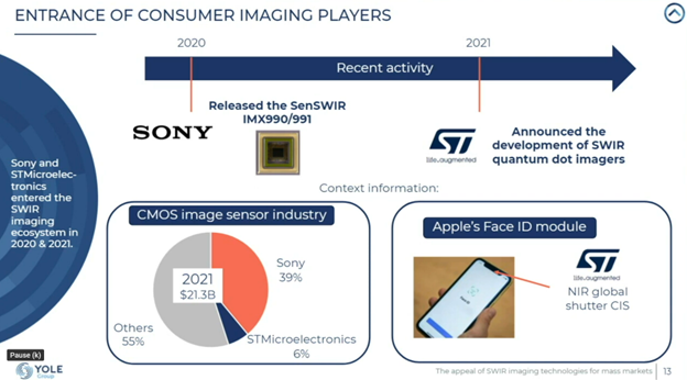
Yole webinar on SWIR applications for consumer markets

Yole published a webinar on SWIR imaging potential applications for mass market:


Friday, December 16, 2022

LiDAR News: Quanergy Files for Bankruptcy

Coverage in Wall Street Journal [paywalled]: https://www.wsj.com/articles/sensor-startup-files-for-bankruptcy-10-months-after-spac-merger-11670975713

From Businesswire: 

Quanergy to Facilitate Sale of Business Through Voluntary Chapter 11 Process, Announces Leadership Changes

SUNNYVALE, Calif.--(BUSINESS WIRE)--Quanergy Systems, Inc. (OTC: QNGY) (“Quanergy” or the “Company”), a leading provider of LiDAR sensors and smart 3D solutions, today announced that the Company initiated an orderly sale process for its business. To facilitate the sale and maximize value, the Company filed for protection under Chapter 11 (“Chapter 11”) of the U.S. Bankruptcy Code (the “Bankruptcy Code”) in the United States Bankruptcy Court for the District of Delaware (the “Bankruptcy Court”) and intends to pursue a sale of the business under section 363 of the Bankruptcy Code.

Quanergy also announced today that Kevin Kennedy, Chief Executive Officer, will retire effective December 31, 2022, but will continue to serve as non-executive Chair of the Board of Directors. Mr. Kennedy will transition executive leadership to a newly appointed Chief Restructuring Officer and President, Lawrence Perkins.

“It has been my honor to serve as CEO at Quanergy for the past 2.5 years,” said Kevin Kennedy, Chief Executive Officer of Quanergy. “During this time, the company shifted our technology focus towards security and industrial applications which enabled the company to grow revenue by serving customer needs in a new marketplace. The Board and I have agreed that it is an appropriate time for me to transition day-to-day leadership to our capable newly appointed Chief Restructuring Officer. I will continue to provide guidance, continuity, and support as non-executive Board Chair.”

Mr. Perkins is the founder and Chief Executive Officer of SierraConstellation Partners, an interim management and advisory firm, which he founded in 2013. Mr. Perkins has served in a variety of senior-level positions, including interim CEO/President, Chief Restructuring Officer, board member, financial advisor, strategic consultant, and investment banker, to numerous private and public middle-market companies.

Prior to the filing of the Company’s Chapter 11 case, the Board of Directors and management evaluated a wide range of strategic alternatives to maximize value for all stakeholders. The Company also significantly reduced operating expenses and resolved significant patent litigation with Velodyne. Now with the protections afforded by the Bankruptcy Code, the Company intends to broaden its marketing efforts to potential purchasers interested in specific business segments or assets as well as continuing to seek a going concern sale of the business.

The Company expects to continue operations during the Chapter 11 process and seeks to complete an expedited sale process with Bankruptcy Court approval. To help fund and protect its operations, Quanergy intends to use available cash on hand along with normal operating cash flows to fund post-petition operations and costs in the ordinary course.

“Quanergy has made considerable efforts to address ongoing financial challenges stemming from volatile capital market conditions,” said Lawrence Perkins, Chief Restructuring Officer and President of Quanergy. “Despite these challenges, the Company has seen improving demand in the security, smart spaces, and industrial markets, and improvements in supply chain conditions. We are confident that Quanergy’s efforts have positioned the Company for a value-maximizing transaction during the Chapter 11 sale process. During the process, we will continue to prioritize the needs of our customers and I am thankful to the entire Quanergy team for their continued efforts and contributions to the business.”

The Company has filed customary motions with the Bankruptcy Court intended to allow Quanergy to maintain operations in the ordinary course including, but not limited to, paying employees and continuing existing benefits programs, meeting commitments to customers and fulfilling go-forward obligations, including vendor payments. Such motions are typical in the Chapter 11 process and Quanergy anticipates that they will be heard in the first few days of its Chapter 11 case.

For more information about the Company’s Chapter 11 case, including claims information, please visit https://cases.stretto.com/Quanergy or call our hotline at 855-613-0451 (for toll-free U.S. and Canada calls) or 949-889-0181 (for tolled international calls).

Cooley LLP is serving as counsel, Young Conaway Stargatt & Taylor LLP is serving as co-counsel, Raymond James & Associates, Inc. is serving as investment banker, and FTI Consulting is serving as financial advisor to Quanergy.

Thursday, December 15, 2022

CES 2023 Award for Aeva Aeries II 4D LiDAR

From Businesswire: 


MOUNTAIN VIEW, Calif.--(BUSINESS WIRE)--Aeva® (NYSE: AEVA), a leader in next-generation sensing and perception systems, today announced that its Aeries™ II sensor has been named a CES® 2023 Innovation Awards Honoree. The prestigious CES Innovation Awards honor outstanding design and engineering in consumer technology products, and were given in advance of CES 2023.

The CES Innovation Award builds on growing recognition for Aeries II and its innovative 4D LiDAR™ technology, which were recently chosen as one of TIME’s Best Inventions of 2022.

“Our next-generation 4D LiDAR technology goes beyond legacy 3D LiDAR systems because of its unique instant velocity detection and long range performance capabilities, in addition to Ultra Resolution,” said Mina Rezk, Co-Founder and CTO at Aeva. “We are honored that Aeries II continues to receive further recognition with this CES Innovation Award because, put simply, we believe Aeva 4D LiDAR has the potential to change the game for passenger cars, commercial vehicles and robotaxis by making vehicle automation safer and more reliable.”

Aeva’s Aeries II 4D LiDAR sensor delivers breakthrough sensing and perception performance using Frequency Modulated Continuous Wave (FMCW) technology to directly detect the instant velocity of each point, in addition to precise 3D position at long range. Its capabilities go beyond legacy time-of-flight 3D LiDAR sensors to enable the next generation of driver assistance and autonomous vehicle capabilities, including:

  • Instant Velocity Detection: Directly measure velocity for each point of detection, in addition to 3D position, to perceive where things are, and precisely how fast they are moving.
  • Long Range Performance: Detect, classify and track objects such as vehicles, cyclists and pedestrians at long distances.
  • Ultra Resolution™: A real-time camera-level image providing up to 20 times the resolution of legacy time-of-flight LiDAR sensors.
  • Road Hazard Detection: Detect small objects on the roadway with greater confidence at up to twice the distance of legacy time-of-flight LiDAR sensors.
  • 4D Localization™: Per-point velocity data enables real-time vehicle motion estimation with six degrees of freedom to enable accurate vehicle positioning and navigation without the need for additional sensors, like IMU or GPS.

Aeries II is the first sensor on the market to integrate Aeva’s unique LiDAR-on-chip technology which integrates all key sensor components including transmitters, receivers and optics onto silicon photonics in a compact module. This design uses no fiber optics, resulting in a highly automated manufacturing process that allows Aeva to scale deployment of its products and lower costs to meet the needs of automotive OEMs and other volume customers.

Detailed information about the CES 2023 Innovation Awards honorees can be found at CES.tech/innovation. In January 2023, Aeva will join other honorees to display their products in the Innovation Awards Showcase area at CES 2023. At the Aeva Booth (#6001, LVCC – West Hall), Aeva will showcase its Aeries II 4D LiDAR sensor alongside its unique LiDAR-on-chip technology that integrates all key LiDAR components onto a silicon photonics chip in a compact module.

Wednesday, December 14, 2022

EETimes article on sensor fusion for neuromorphic vision

Link: https://www.eetimes.com/improving-sensor-fusion-for-neuromorphic-vision/

Improving Sensor Fusion for Neuromorphic Vision (Nov 21, 2022)

The article links two videos about event cameras. The first one is a tutorial about event cameras from 2020:


The second video shows an example of a commercially available event camera called Davis camera (made by iniVation AG) which has a CMOS image sensor together with an event sensor and allows sensor fusion, giving the best of both worlds:


The article ends by highlighting two key challenges for wider applicability of event-based image sensors: (1) non-standard processing techniques that are different form conventional RGB data processing pipelines, (2) high power requirements of event data processing schemes.

Monday, December 12, 2022

"Burst Vision" using SPAD Cameras

In a paper titled "Burst Vision Using Single-Photon Cameras", Sizhuo Ma, Paul Mos, Edoardo Charbon and Mohit Gupta from University of Wisconsin-Madison and École polytechnique fédérale de Lausanne write:

Single-photon avalanche diodes (SPADs) are novel image sensors that record the arrival of individual photons at extremely high temporal resolution. In the past, they were only available as single pixels or small-format arrays, for various active imaging applications such as LiDAR and microscopy. Recently, high-resolution SPAD arrays up to 3.2 megapixel have been realized, which for the first time may be able to capture sufficient spatial details for general computer vision tasks, purely as a passive sensor. However, existing vision algorithms are not directly applicable on the binary data captured by SPADs. In this paper, we propose developing quanta vision algorithms based on burst processing for extracting scene information from SPAD photon streams. With extensive real-world data, we demonstrate that current SPAD arrays, along with burst processing as an example plug-and-play algorithm, are capable of a wide range of downstream vision tasks in extremely challenging imaging conditions including fast motion, low light ($<5$ lux) and high dynamic range. To our knowledge, this is the first attempt to demonstrate the capabilities of SPAD sensors for a wide gamut of real-world computer vision tasks including object detection, pose estimation, SLAM, and text recognition. We hope this work will inspire future research into developing computer vision algorithms in extreme scenarios using single-photon cameras.


Full paper is available here: https://wisionlab.com/wp-content/uploads/2022/11/burst_vision_wisionlab.pdf

The paper will be presented at the upcoming Winter Conference on Applications of Computer Vision (WACV) conference in January 2023. 


Video summary


Dealing with motion blur in extremely low light


Dealing with extreme dynamic range


A large dataset of over 50 million binary burst frames for a wide range of computer vision tasks


Friday, December 09, 2022

Global CMOS Image Sensor Market to Grow at 6.32% CAGR, Expected to Reach USD 39.54 Billion by 2031

Link: https://www.gophotonics.com/news/details/3480-global-cmos-image-sensor-market-to-grow-at-6-32-cagr-expected-to-reach-usd-39-54-billion-by-2031


Research Nester recently published a report on "CMOS Image Sensor Market Analysis by Technology; and by End Use Industry – Global Supply & Demand Analysis & Opportunity Outlook 2018-2031."

The Global CMOS Image Sensor Market is estimated to grow at a CAGR of 6.32% over the forecast period, i.e., 2022-2031. Rising demand for high-definition image-capturing devices is expected to propel the market growth. For instance, Sony Corporation unveiled the IMX485 type 1/1.2 4K-resolution back-illuminated CMOS image sensor and the IMX415 type 1/2.8 4K CMOS image sensor in June 2019. Sony created these two security camera sensors to address the constantly growing demand for security cameras in a range of monitoring applications, such as anti-theft, disaster warning, and traffic monitoring systems, or commercial complexes.

Furthermore, there has been growing demand for CMOS image sensor in healthcare industry. They are usually used in observing patient during the surgeries. A recent report by the National Library of Medicine states that a staggering 310 million major procedures are carried out year around the world, with between 40 to 50 million taking place in the United States and 20 million in Europe.

Global CMOS Image Sensor Market: Key Takeaways

  •  Asia Pacific to hold the largest market revenue
  •  Popularity of smartphones to propel market growth in North America region
  •  Consumer electronics segment to garner the largest revenue


Rising Demand for Security & Surveillance to Drive Market Growth
CMOS image sensor is extensively used for the purpose of security and surveillance. CMOS image sensor has an ability to convert the photoelectrical signal into digital signal. Security is the major concern for everyone. Hence owing to increasing instances of theft and crime, more security cameras having CMOS senor are expected to be installed, allowing market growth. As it is estimated that approximately 82% of burglars check the presence of alarm system before breaking in.
However, they can’t be installed everywhere owing to privacy concerns. Hence many organizations have come up with innovative ideas which are anticipated to fuel the market. For instance, in December 2021, Canon revealed a brand-new outdoor 4K camera that can be used as both a conventional camera and a security camera. Additionally, it can combine every 4K UHD pixel that the 4K UHD CMOS image sensor has ever captured.

Global CMOS Image Sensor Market: Regional Overview
The global CMOS image sensor market is segmented into five major regions including North America, Europe, Asia Pacific, Latin America, and the Middle East and Africa region.
Government Initiative for Smart Cities to Drive Growth in Asia Pacific Region
The CMOS image sensor market in Asia Pacific region is anticipated to garner the largest revenue of USD 17,759.3 Million by the end of 2031. Government initiatives for smart cities is expected to fuel the growth in the market. The Ministry of Electronics and Information Technology in India has tasked ERNET India and IISc with developing the LoRa gateway (pole gateway), a low-cost compute device that can connect to cameras, temperature, humidity, air quality, and other sensors. This is part of the

Internet of Things (IoT) Management Framework for Smart Cities.
Growing Demand for Consumer Electronics to Favour Growth in North America Region
Further, North America Region is expected to grow further by garnering revenue of USD 12579.0 Million by the end of 2031, growing at a CAGR of 6.14% during 2022-2031. Increase in demand for smartphones to drive the market growth. Approximately 85% percent of all mobile users in the US are expected to have a smartphone by 2025. Various electronics item including smart phones, TVs, wearable gadgets and more consist of senor which is in huge demand in this region. Many smartphones manufacturers use image sensor in their smartphones. For instance, the Xiaomi 12S Ultra smartphone contains the world's biggest sensor in a smartphone. As part of the new line, Xiaomi has launched the 12S Series, which includes the Leica-engineered Ultra.
The study further incorporates Y-O-Y growth, demand & supply and forecast future opportunity in:

  •  North America (U.S., Canada)
  •  Europe (U.K., Germany, France, Italy, Spain, Hungary, Belgium, Netherlands & Luxembourg, NORDIC [Finland, Sweden, Norway, Denmark], Poland, Turkey, Russia, Rest of Europe)
  •  Latin America (Brazil, Mexico, Argentina, Rest of Latin America)
  •  Asia-Pacific (China, India, Japan, South Korea, Indonesia, Singapore, Malaysia, Australia, New Zealand, Rest of Asia-Pacific)
  •  Middle East and Africa (Israel, GCC [Saudi Arabia, UAE, Bahrain, Kuwait, Qatar, Oman], North Africa, South Africa, Rest of Middle East and Africa).
  • Global CMOS Image Sensor Market, Segmentation by End Use Industry
  •  Consumer Electronics
  •  Medical
  •  Industrial
  •  Security & Surveillance
  •  Automotive & Transportation
  •  Aerospace & Defense

The consumer electronics segment is estimated to hold the largest revenue of USD 27010.4 Million by the end of 2031. Increasing demand for CMOS in consumer electronics is expected to boost the market growth. This CMOS technology is extensively used in smartphones. CMOS are known for using less power and hence their demand in smartphones are increasing. Instead of capturing the whole image in a single instance it captures image in scanning type way. Moreover, cameras with CMOS sensor gives better saturation capacity owing to which many manufacturers are installing it in their smartphones. For instance, the newest CMOS image sensor in the XGS series was unveiled by ON Semiconductor. A 16Mp sensor called the XGS 16000 offers excellent global shutter imaging for robotics and inspection systems in factories. The XGS 16000 delivers great performance at low power while giving the highest resolutions for typical 29 x 29 mm industrial cameras, consuming just 1 Watt at 65FPS. In North America, the segment generated the largest revenue of USD 8576.4 Million by the end of 2031, while in the Asia Pacific, the segment is projected to register the largest revenue of USD 12124.3 Million by the end of 2031.

Global CMOS Image Sensor Market, Segmentation by Technology

  •  Front Side Illumination (FSI)
  •  Back Side Illumination (BSI)

The back side illumination (BSI) segment is anticipated to garner the largest revenue by the end of 2031, growing at the highest CAGR of 6.68% over the forecast period. The growth can be attributed to the increasing use of BSI technology in high quality and higher pixel cameras. The preference of smartphones producer is increasing for BSI technology which is also expected to lead a boost in demand. For instance, with the 42 megapixel Sony Alpha A7R Mark II, Sony has added a BSI Full-Frame sensor. The Sony Cyber-shot RX10 II and RX100 IV both have "stacked" sensors that enable even faster continuous shooting and high speed video recording. In the Asia Pacific, the segment is projected to grow with a CAGR of 7.34% during the forecast period, while in North America, the front side illumination (FSI) segment is projected to grow with a CAGR of 5.41% during the forecast period.
Few of the well-known market leaders in the global CMOS image sensor market that are profiled by Research Nester are STMicroelectronics International NV, Samsung Electronics America, Inc., Sony Semiconductor Solutions Corporation, ON Semiconductor Components Industries, LLC, Canon, Inc., SK Hynix Inc., OMNIVISION Technologies Inc., Hamamatsu Photonics K.K., Panasonic Industry Co. Ltd., and Teledyne Technologies Inc. and other key players.

Recent Development in in the Global CMOS Image Sensor Market

In December 15, 2021, Canon creates the world's highest resolution 3.2 megapixel SPAD sensor and introduces a breakthrough low-light imaging camera that achieves outstanding colour reproduction even in dimly lit conditions.

In February 14, 2018, Panasonic Corporation revealed that it has created a breakthrough technology that enables simultaneous 450k high-saturation electrons, global shutter photography with sensitivity modulation, and 8K high-resolution (36M pixels) imaging using a CMOS image sensor with an organic photoconductive layer (OPF).

Wednesday, December 07, 2022

Videos of the day [AMS-OSRAM, ESPROS, Sony]

New Mira global shutter image sensor from ams OSRAM advances 2D and 3D sensing with high quantum efficiency at visible and NIR wavelengths. The Mira sensors come supplied in a chip-scale package, with an optimized footprint and an industry-leading ratio of size to resolution empowered by state-of-the-art stacked back-side illumination technology to shrink package footprint, giving greater design flexibility to manufacturers of smart glasses and other space-constrained products. The Mira image sensors are super small and offer superior image quality in low light conditions and with its many on-chip operations, our image sensors open up many new possibilities for developers.


Monday, December 05, 2022

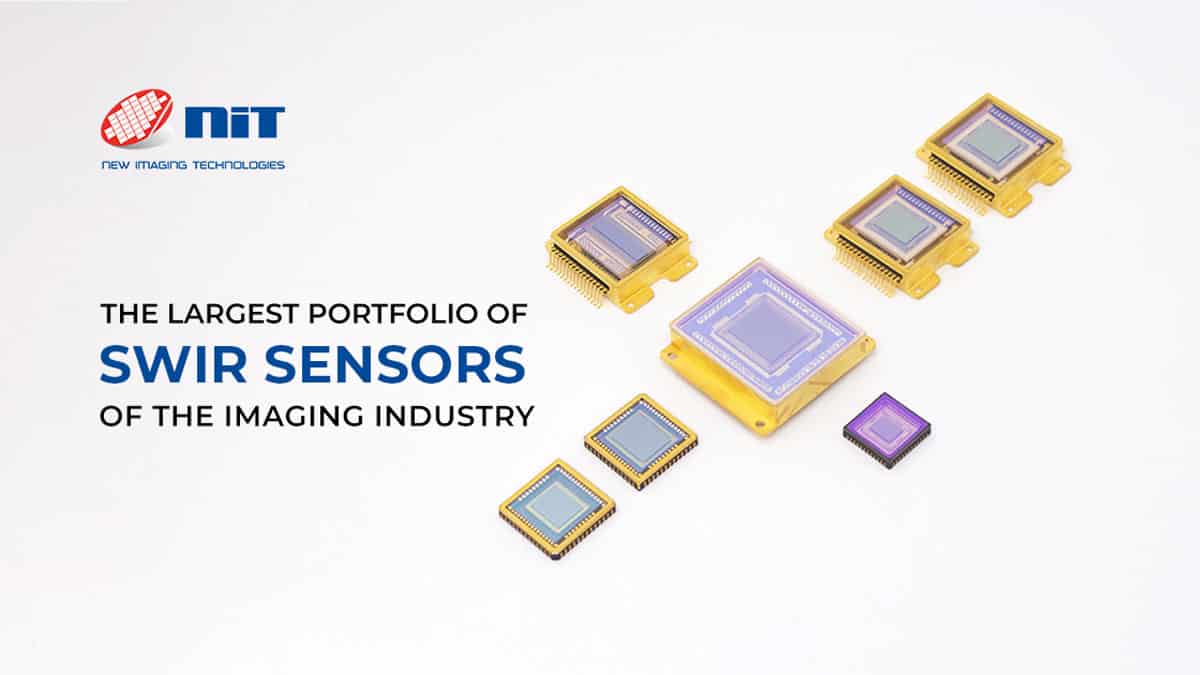
NIT SWIR Portfolio

Press release from NIT (New Imaging Technologies) about their wide range of SWIR offerings:

https://new-imaging-technologies.com/news/the-largest-portfolio-of-swir-sensors-of-the-imaging-industry/


NIT is widely known for its large range of SWIR cameras designed for industrial, defense, and medical markets. Less known is that NIT designs and manufactures in-house all the InGaAs sensors embedded into our cameras. We master the design of silicon read-out circuits, InGaAs photodiode arrays, and assembly technologies such as 3D stacking.

Our recent investment into a new clean room facility and back-end process machines will bring our production capacity to several ten thousand sensors per year with the highest quality. ​


Such vertical integration allows us to offer a line of cameras with specific features, all adapted to our customer markets and applications. Our cameras and their performances are unique as they don’t use third-party sensors. The sensitivity, noise level, frame rate, pitches, dynamic range, and pixel numbers of our InGaAs sensors make our cameras the best in their class.​