Tuesday, January 31, 2023

Registrations Open for Harvest Imaging Forum (Apr 5-6, 2023)

When: April 5 and 6, 2023
Where: Delft, the Netherlands
Forum Topic: Imaging Beyond the Visible
Speaker: Prof. dr. Pierre Magnan (ISAE-SUPAERO, France)
Registration link: https://harvestimaging.com/forum_registration_2023_new.php

More information can be found here: https://harvestimaging.com/forum_introduction_2023_new.php

After the Harvest Imaging forums during the last decade, a next and ninth one will be organized on April 5 & 6, 2023 in Delft, the Netherlands. The basic intention of the Harvest Imaging forum is to have a scientific and technical in-depth discussion on one particular topic that is of great importance and value to digital imaging. The forum 2023 will again be organized in a hybrid form:

  • You can attend in-person and can benefit in the optimal way of the live interaction with the speakers and audience,
  • There will be also a live broadcast of the forum, still interactions with the speakers through a chat box will be made possible,
  • Finally the forum also can be watched on-line at a later date.

The 2023 Harvest Imaging forum will deal with a single topic from the field of solid-state imaging and will have only one world-level expert as the speaker.

Register here: https://harvestimaging.com/forum_registration_2023_new.php


"Imaging Beyond the Visible"
Prof. dr. Pierre MAGNAN (ISAE-SUPAERO, Fr)
 

Abstract:
Two decades of intensive and tremendous efforts have pushed the imaging capabilities in the visible domain closer to physical limits. But also extended the attention to new areas beyond visible light intensity imaging. Examples can be found either to higher photon energy with appearance of CMOS Ultra-Violet imaging capabilities or even to other light dimensions with Polarization Imaging possibilities, both in monolithic form suitable to common camera architecture.

But one of most active and impressive fields is the extension of interest to the spectral range significantly beyond the visible, in the Infrared domain. Special focus is put on the Short Wave Infrared (SWIR) used in the reflective imaging mode but also the Thermal Infrared spectral range used in self-emissive ‘thermal’ imaging mode in Medium Wave Infrared (MWIR) and Long Wave Infrared (LWIR). Initially mostly motivated for military and scientific applications, the use of these spectral domains have now met new higher volume applications needs.

This has been made possible thanks to new technical approaches enabling cost reduction stimulated by the efficient collective manufacturing process offered by the microelectronics industry. CMOS, even no more sufficient to address alone the non- visible imaging spectral range, is still a key part of the solution.

The goal of this Harvest Imaging forum is to go through the various aspects of imaging concepts, device principles, used materials and imager characteristics to address the beyond-visible imaging and especially focus on the infrared spectral bands imaging.

Emphasis will be put on the material used for both detection :

  • Germanium, Quantum Dots devices and InGaAs for SWIR,
  •  III-V and II-VI semiconductors for MWIR and LWIR
  •  Microbolometers and Thermopiles thermal imagers

Besides the material aspects, also attention will be given to the associated CMOS circuits architectures enabling the imaging arrays implementation, both at the pixel and the imager level.
A status on current and new trends will be provided.
 

Bio:
Pierre Magnan graduated in E.E. from University of Paris in 1980. After being a research scientist involved in analog and digital CMOS design up to 1994 at French Research Labs, he moved in 1995 to CMOS image sensors research at SUPAERO (now ISAE-SUPAERO) in Toulouse, France. The latter is an Educational and Research Institute funded by the French Ministry of Defense. Here Pierre was involved in setting up and growing the CMOS active-pixels sensors research and development activities. From 2002 to 2021, as a Full Professor and Head of the Image Sensor Research Group, he has been involved in CMOS Image Sensor research. His team worked in cooperation with European companies (including STMicroelectronics, Airbus Defense& Space, Thales Alenia Space and also European and French Space Agencies) and developed custom image sensors dedicated to space instruments, extending in the last years the scope of the Group to CMOS design for Infrared imagers.
In 2021, Pierre has been nominated Emeritus Professor of ISAE-Supaero Institute where he focuses now on Research within PhD work, mostly with STMicroelectronics.

Pierre has supervised more than 20 PhDs candidates in the field of image sensors and co-authored more than 80 scientific papers. He has been involved in various expertise missions for French Agencies, companies and the European Commission. His research interests include solid-state image sensors design for visible and non-visible imaging, modelling, technologies, hardening techniques and circuit design for imaging applications.

He has served in the IEEE IEDM Display and Sensors subcommittee in 2011-2012 and in the International Image Sensor Workshop (IISW) Technical Program Committee, being the General Technical Chair of 2015 IISW. He is currently a member of the 2022 IEDM ODI sub-committee and the IISW2023 Technical Program Committee.

Monday, January 30, 2023

Samsung Tech Blog about ISOCELL Color, HDR and ToF Imaging

Link: https://semiconductor.samsung.com/newsroom/tech-blog/how-isocell-unlock-the-future-of-camera-experiences/

Some excerpts below.

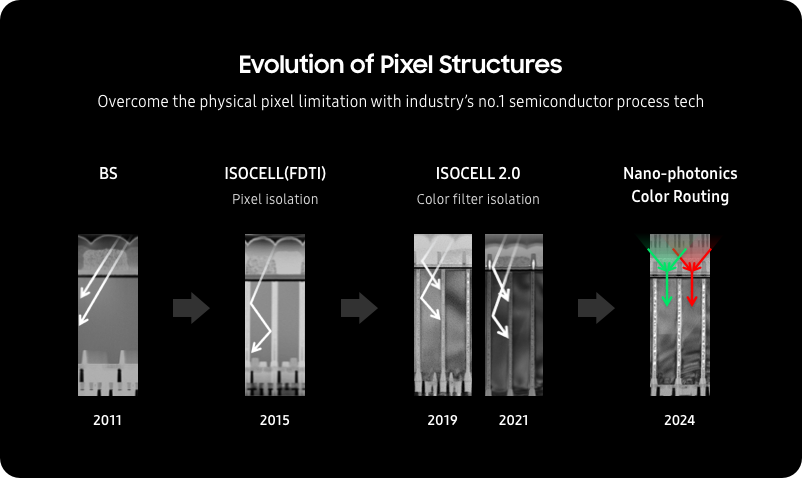
The science of creating pixels has made substantial progress in recent years. As a rule, high resolution image sensors need small, light-sensitive pixels. To capture as much light as possible, the pixel structure has evolved from front-side illumination (FSI) to a back-side illumination (BSI). This places the photodiode layer on top of the metal line, rather than below it. By locating the photodiode closer to the light source, each pixel is able to capture more light. The downside of this structure is that it creates higher crosstalk between the pixels, leading to color contamination.

“To remedy such a drawback, Samsung introduced ISOCELL, its first technology that isolates pixels from each other by adding barriers. The name ISOCELL is a compound word from the words “isolate’ and ‘cell,’” Kim explained. “By isolating each pixel, ISOCELL can increase a pixel’s full well capacity to hold more light and reduce crosstalk from one pixel to another.”


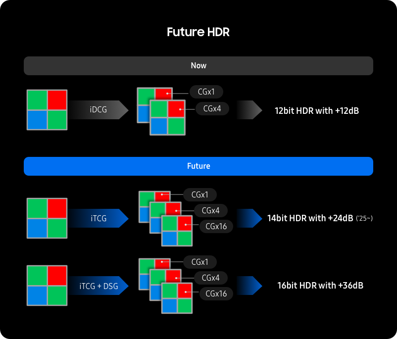
With ISOCELL technology, ISOCELL image sensors have very high full well capacity. Pixels in the newest ISOCELL image sensor have up to 70,000 electrons, allowing the sensor to reach huge signal range.  ... “To reduce noise, we perform two readouts: One with high gain to show the dark details and another with low gain to show the bright details. The two readouts are then merged in the sensor. Each read out has 10-bits. With the high conversion gain readout at 4x, it adds an additional 2-bits, producing 12-bit HDR image output. This technology is called Smart-ISO Pro also known as iDCG (intra-scene Dual Conversion Gain).”


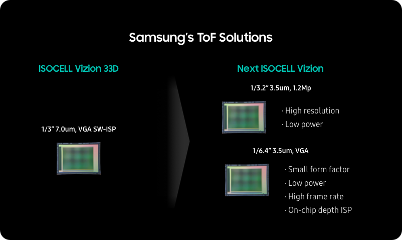
Samsung has a plan to release a new generation of iToF sensor that has an image signal processor (ISP) integrated. The whole processing of depth information is done on the ISP within the sensor, rather than delegating to the SoC, so that the overall operation uses lower power consumption. In addition, the new solution offers improved depth quality even in scenarios such as low light environment, narrow objects or repetitive patterns. For future applications, Samsung’s ISP integrated ToF will help provide high quality depth image with little to no motion blur or lagging, at a high frame rate.


SD Optics releases MEMS-based system "WiseTopo" for 3D microscopy

SD Optics has released WiseTopo, a MEMS-based microarray lens system that transforms a 2D microscopes into 3D. 
 
Attendees at Photonics West can see a demonstration at their booth #4128 between Jan 31 to Feb 2, 2023 at the Moscone Center in San Francisco, California.


SD OPTICS introduces WiseTopo with our core technology Mals lens, the Mems-based microarray lens system. WiseTopo transforms a 2D microscope into a 3D microscope with a simple plug-in installation, and it fits all microscopes. The conventional system has a limited depth of field, so a user has to adjust the focus manually by moving the z-axis. It is difficult to identify the exact shape of the object instantly.  The manual movements can cause deviations in the observation, missing information, incomplete inspection, and an increase in user work load. SD Optics' WiseTopo is the most innovative 3D microscope module empowered with the patented core technology Mals. WiseTopo converts a 2D microscope into a 3D microscope by replacing the image sensor. With this simple installation, WiseTopo resolves the depth-of-field issue without Z-axis movement. Mals is an optical Mems-based, ultra-fast variable focusing lens that implements curvature changes in the lens with the motion of individual micro-mirrors. Mals moves and focuses at a speed of 12Khz without z-axis mechanical movement. It is a semi-permanent digital lens technology that operates at any temperature and has no life cycle limit. WiseTopo provides ideal features in combination with our developed software. These features let users have a better understanding of an object in real time. WiseTopo provides an All-in-focus function where everything is in focus. The Auto-focus function automatically focuses on the Region of Interest Focus lock maintains focus when multiple focus ROIs are set in the z-axis, multi-focus lock stays in focus even when moving the X- and Y-axis. Auto-focus lock retains auto-focus during Z-axis movement and others. These functions maximize user convenience. WiseTopo and its 3D images will reveal necessary information that is hidden when using a 2D microscope. WiseTopo obtains in-focused images with fast varying focus technology and processes many 3D attributes such as shape matching and point cloud instantly. WiseTopo supports various 3D data formats for analysis. For example, a comparison between the reference 3D data with the real-time 3D data can be performed easily. In the microscope, objective lenses with different magnifications are mounted on the turret. Wisetopo provides all functions even when the magnification is changed. Wisetopo provides all 3D features in any microscope and can be used with all of them, regardless of the brand
3D images created in Wisetopo can be viewed in AR/VR. This will let users feel and observe 3D data in the metaverse space.
 

Friday, January 27, 2023

poLight’s paper on passive athermalisation of compact camera/lens using its TLens® tunable lens

Images defocus over wide temperature range is a challenge in many applications. poLight's TLens technology behaves the opposite of plastic lenses over temperature, so just adding it to the optics stack addresses this issue.

A whitepaper is available here: [link]

Abstract: poLight ASA is the owner of and has developed the TLens products family as well as other patented micro-opto-electro-mechanical systems (MOEMS) technologies. TLens is a focusable tunable optics device based on lead zirconium titanate (PZT) microelectromechanical systems (MEMS) technology and a novel optical polymer material. The advantages of the TLens have already been demonstrated in multiple products launched on the market since 2020. Compactness, low power consumption, and fast speed are clear differentiators in comparison with incumbent voice coil motor (VCM) technology, thanks to the patented MEMS architecture. In addition, the use of TLens in the simple manner by adding it onto a fixed focus lens camera, or inserting the TLens inside the lens stack, enables stable focusing over an extended operating range. It has been demonstrated that the TLens passively compensates the thermal defocus of the plastic lens stack/camera structure. The fixed focus plastic lens stack cameras, usually used in consumer devices, typically exhibits a thermal defocus of a few diopters over the operating temperature range. Results of simulations as well as experimental data are presented together with a principal athermal lens design using TLens in only a passive manner (without the use of its electro-tunablity) while the electro-tunability can be used to additionally secure an extended depth of focus with further enhanced image quality.


Thursday, January 26, 2023

Towards a Colorimetric Camera - Talk from EI 2023 Symposium

Tripurari Singh and Mritunjay Singh of Image Algorithmics presented a talk titled "Towards a Colorimetric Camera" at the recent Electronic Imaging 2023 symposium. They show that for low-light color imaging it is better to use a long/medium/short (LMS) filter that more closely mimics human color vision as opposed to the traditional RGB Bayer pattern.


Wednesday, January 25, 2023

Jabil Inc. collaboration with ams OSRAM and Artilux

Link: https://www.jabil.com/news/swir-3d-camera-prototype.html

ST. PETERSBURG, FL – January 18, 2023 – Jabil Inc. (NYSE: JBL), a leading manufacturing solutions provider, today announced that its renowned optical design center in Jena, Germany, is currently demonstrating a prototype of a next-generation 3D camera with the ability to seamlessly operate in both indoor and outdoor environments up to a range of 20 meters. Jabil, ams OSRAM and Artilux combined their proprietary technologies in 3D sensing architecture design, semiconductor lasers and germanium-silicon (GeSi) sensor arrays based on a scalable complementary metal-oxide-semiconductor (CMOS) technology platform, respectively, to demonstrate a 3D camera that operates in the short-wavelength infrared (SWIR), at 1130 nanometers.

Steep growth in automation is driving performance improvements for robotic and mobile automation platforms in industrial environments. The industrial robot market is forecast to grow at over 11% compound annual growth rate to over $35 billion by 2029. The 3D sensor data from these innovative depth cameras will improve automated functions such as obstacle identification, collision avoidance, localization and route planning — key applications necessary for autonomous platforms. 

“For too long, industry has accepted 3D sensing solutions limiting the operation of their material handling platforms to environments not impacted by the sun. The new SWIR camera provides a glimpse of the unbounded future of 3D sensing where sunlight no longer impinges on the utility of autonomous platforms,” said Ian Blasch, senior director of business development for Jabil’s Optics division. “This new generation of 3D cameras will not only change the expected industry standard for mid-range ambient light tolerance but will usher in a new paradigm of sensors capable of working across all lighting environments.”

“1130nm is the first of its kind SWIR VCSEL technology from ams OSRAM, offering enhanced eye safety, outstanding performance in high sunlight environments, and skin detection capability, which is of critical importance for collision avoidance when, for example humans and industrial robots interact,” says Dr. Joerg Strauss, senior vice president and general manager at ams OSRAM for business line visualization and sensing. “We are excited to partner with Jabil to make the next-generation 3D sensing and machine vision solutions a reality.”

Dr. Stanley Yeh, vice president of platform at Artilux, concurs, “We are glad to work with Jabil and ams OSRAM to deliver the first mid-range SWIR 3D camera with the use of near infrared (NIR)-like components such as CMOS-based sensor and VCSEL. It's a significant step toward the mass-adoption of SWIR spectrum sensing and being the leader of CMOS SWIR 2D/3D imaging technology.”
For nearly two decades, Jabil’s optical division has been recognized by leading technology companies as the premier service provider for advanced optical design, industrialization and manufacturing. Our Optics division has more than 170 employees across four locations. Jabil’s optics designers, engineers and researchers specialize in solving complex optical problems for its customers in 3D sensing, augmented and virtual reality, action camera, automotive, industrial and healthcare markets. Additionally, Jabil customers leverage expertise in product design, process development, testing, in-house active alignment (from Kasalis, a technology division of Jabil), supply chain management and manufacturing expertise.

More information and the test data could be found at the following website: www.jabil.com/3DCamera


Tuesday, January 24, 2023

CIS market news 2022/2023

Recent Will Semi report that includes some news about Omnivision (Howell): https://tech.ifeng.com/c/8MXij5vF1lP

It is worth noting that in December 2022, Howell Group, a subsidiary of Weir, issued an internal letter announcing cost control, with the goal of reducing costs by 20% by 2023.

In an internal letter, Howell Group said, "The current market situation is very serious. We are facing great market challenges, and prices, inventory and supply chains are under great pressure. Therefore, we must carry out cost control, with the goal of reducing costs by 20% by 2023.

In order to achieve this goal, Howell Group also announced: stop all recruitments and leave without substitutes; salary cuts for senior managers; stop work during the Spring Festival in all regions of the group; quarterly bonuses and any other form of bonuses will be discontinued; expenditure strictly controlled; and some R&D projects will also reduce NRE expenditure.

Howell Group said, "These measures are temporary, and we believe that business-level improvements will occur in the second half of next year, because we have a new product layout in the consumer market, while automobiles and emerging markets are rising steadily. We will reassess the situation at the end of the first quarter of next year (2023). 


More related news from Counterpoint Research: : https://www.counterpointresearch.com/global-smartphone-cis-market-revenues-shipments-dip-2022/

Global Smartphone CIS Market Revenues, Shipments Dip in 2022

  • In 2022, global smartphone image sensor shipments were estimated to drop by mid-teens YoY.
  • Global smartphone image sensor revenues were down around 6% YoY during the year.
  • Sony was the only major vendor to achieve a YoY revenue growth, thanks to Apple’s camera upgrades.
  • Both Sony and Samsung managed to improve their product mix.

Compare Omnivision sales with its peers in this graphic:


Thursday, January 19, 2023

European Defense Fund project for next gen IR sensors

From Wiley industry news: https://www.wileyindustrynews.com/en/news/eu19m-project-set-enable-next-generation-ir-sensors

€19M project set to enable next-generation IR sensors

13.01.2023 - A four-year defense project, led by Lynred, is first to see EU infrared product manufacturers jointly acquire access to advanced CMOS technology to design new infrared sensors.
A ten-member consortium aims to gain European sovereignty in producing highperformance IR sensors for future defense systems. Lynred, a French provider of high-quality infrared detectors for the aerospace, defense and commercial markets, leads HEROIC, a European Defence Fund project aimed at developing highlyadvanced electronic components for next-generation infrared (IR) sensors, while consolidating the supply chain of these state-of-the-art products in Europe.

High Efficiency Read-Out Integrated Circuit (HEROIC) is a four-year project starting January 2023 with a budget in the order of 19 million euros, of which the European Defence Fund is contributing €18M. 
 
HEROIC is the first collaboration of its kind to bring together European IR manufacturers, several of whom are competitors, to strategically tackle a common problem. The project’s main objectives are to increase access to, and dexterity in, using a new European-derived advanced CMOS technology that offers key capabilities in developing the next generations of high-performance infrared sensors – these will feature smaller pixels and advanced functions for defense applications. One overall aim is to enable Europe to gain technological sovereignty in producing high-performance IR sensors.
 
Consortium members include three IR manufacturers: AIM (DE), project leader Lynred (FR), and Xenics (BE); four system integrators: Indra (ES), Miltech Hellas (GR), Kongsberg (NO) and PCO SA (PL); a component provider: Ideas, an IC developer (NO), as well as two research institutions CEA-Leti (FR), and the University of Seville (ES).
 
“Lynred is proud to collaborate on this game-changing project aimed at securing European industrial sovereignty in the design and supply of IR sensors,” said David Billon-Lanfrey, chief strategy officer at Lynred. “This project represents the first phase for European IR manufacturers to gain access to a superior CMOS technology compatible with various IR detectors and 2D/3D architectures, and equally importantly, make it available within a robust EU supply chain.”

Acquiring the latest advanced CMOS technology with a node that no consortium partner has had an opportunity to access is pivotal to the sustainable design of a next-generation read-out integrated circuit (ROIC). Its commonly specified platform will allow each consortium partner to pursue its respective technological roadmap and more effectively meet the higher performance expectations of post-2030 defense systems.

“The HEROIC project will enable AIM to develop advanced ROICs based on European silicon CMOS technology, as an important building block in its next-generation IR sensors,” said Rainer Breiter, vice-president, IR module programs, at AIM. “We are looking forward to working together with our partners in this common approach to access the latest advanced CMOS technology.”

IR sensors are used to detect, recognize and identify objects or targets during the night and in adverse weather and operational conditions. They are at the center of multiple defense applications: thermal imagers, surveillance systems, targeting systems and observation satellites.

Next-generation IR systems will need to exhibit longer detection, recognition and identification ranges, and offer larger fields of view and faster frame rates. This will require higher resolution formats encompassing further reductions in pixel pitch sizes down from today’s standard 15 μm and 10 μm to 7.5 μm and below. This will need to be obtained without increasing the small footprint of the IR sensor, thus maintaining reasonable system costs and mechanical/electrical interfaces. These requirements make the qualification of a new CMOS technology mandatory to achieving higher performance at the IR sensor level.

"Xenics sees the HEROIC project as a cornerstone for its strategy of SWIR development for defense applications,” said Paul Ryckaert, CEO of Xenics. “Thanks to this project, the consortium partners will shape the future of European CMOS developments and technologies for IR sensors.”


Tuesday, January 17, 2023

Videos du Jour Jan 17, 2023: Flexible image sensors, Samsung ISOCELL, Hamamatsu


Flexible Image Sensor Fabrication Based on NIPIN Phototransistors

Hyun Myung Kim, Gil Ju Lee, Min Seok Kim, Young Min Song
Gwangju Institute of Science and Technology, School of Electrical Engineering and Computer Science;

We present a detailed method to fabricate a deformable lateral NIPIN phototransistor array for curved image sensors. The phototransistor array with an open mesh form, which is composed of thin silicon islands and stretchable metal interconnectors, provides flexibility and stretchability. The parameter analyzer characterizes the electrical property of the fabricated phototransistor.


ISOCELL Image Sensor: Ultra-fine Pixel Technologies | Samsung

ISOCELL has evolved to bring ultra-high resolution to our mobile photography. 
Learn more about Samsung's ultra-fine pixel technologies.
http://smsng.co/Pixel_Technologies


Photon counting imaging using Hamamatsu's scientific imaging cameras - TechBites Series

With our new photon number resolving mode the ORCA-Quest enables photon counting resolution across a full 9.4 megapixel image. See the camera in action and learn how photon number imaging pushes quantitative imaging to a new frontier.


Friday, January 13, 2023

Advantages of a one-bit quanta image sensor

In an arXiv preprint, Prof. Stanley Chan of Purdue University writes:

The one-bit quanta image sensor (QIS) is a photon-counting device that captures image intensities using binary bits. Assuming that the analog voltage generated at the floating diffusion of the photodiode follows a Poisson-Gaussian distribution, the sensor produces either a “1” if the voltage is above a certain threshold or “0” if it is below the threshold. The concept of this binary sensor has been proposed for more than a decade and physical devices have been built to realize the concept. However, what benefits does a one-bit QIS offer compared to a conventional multi-bit CMOS image sensor? Besides the known empirical results, are there theoretical proofs to support these findings? The goal of this paper is to provide new theoretical support from a signal processing perspective. In particular, it is theoretically found that the sensor can offer three benefits: (1) Low-light: One-bit QIS performs better at low-light because it has a low read noise and its one-bit quantization can produce an error-free measurement. However, this requires the exposure time to be appropriately configured. (2) Frame rate: One-bit sensors can operate at a much higher speed because a response is generated as soon as a photon is detected. However, in the presence of read noise, there exists an optimal frame rate beyond which the performance will degrade. A Closed-form expression of the optimal frame rate is derived. (3) Dynamic range: One-bit QIS offers a higher dynamic range. The benefit is brought by two complementary characteristics of the sensor: nonlinearity and exposure bracketing. The decoupling of the two factors is theoretically proved, and closed-form expressions are derived.

Pre-print available here: https://arxiv.org/pdf/2208.10350.pdf


The paper argues that, if implemented correctly, there are three main benefits:

1. Better SNR in low light

2. Higher speed (frame rate)

3. Better dynamic range

This paper has many interesting technical results and insights. It provides a balanced view in terms of the regimes where single-photon quanta image sensor provide benefits over conventional image sensors.