STMicroelectronics accelerates global adoption and market growth of Physical AI with NVIDIA
STMicroelectronics to integrate ST sensors, microcontrollers, and motor control solutions with NVIDIA robotics ecosystem to help developers design, train, and deploy humanoid robots and other physical AI systems with higher efficiency, reliability, and scalability
First steps with integration of Leopard Imaging stereo depth camera enabled by ST with the NVIDIA Holoscan Sensor Bridge, and the addition of the high-fidelity sim-to-real model of ST IMU in NVIDIA Isaac Sim ecosystem
STMicroelectronics (NYSE: STM), a global semiconductor leader serving customers across the spectrum of electronics applications, today announced the acceleration of global development and adoption of physical AI systems, including humanoid, industrial, service and healthcare robots. ST is integrating its comprehensive portfolio for advanced robotics, into the reference set of components compatible with the NVIDIA Holoscan Sensor Bridge (HSB). In parallel, high-fidelity NVIDIA Isaac Sim models of ST components are being integrated into both companies’ robotics ecosystems to support faster, more accurate sim-to-real research and development. The first deliverables available to developers today include the integration of Leopard’s depth camera enabled by ST with the NVIDIA HSB and the high-fidelity model of an ST IMU into NVIDIA’s Isaac Sim ecosystem.
“ST is well engaged within the robotics community, providing robust support and a well-established ecosystem,” said Rino Peruzzi, Executive Vice President, Sales & Marketing, Americas & Global Key Account Organization at STMicroelectronics. “Our collaboration with NVIDIA aims to unleash the next wave of cutting-edge robotics innovation with developer and customer experience streamlined at every step, from the inception of AI algorithms to the seamless integration of sensors and actuators. This will accelerate the evolution of sophisticated AI-driven physical platforms.”
“Accelerating the development of next-generation autonomous systems requires high-fidelity simulation and seamless hardware integration to bridge the gap between virtual training and real-world deployment,” said Deepu Talla, Vice President of Robotics and Edge AI at NVIDIA. “The integration of STMicroelectronics’ sensor and actuator technologies with NVIDIA Isaac Sim, Holoscan Sensor Bridge and Jetson platforms provides developers with a unified foundation to build, simulate and deploy physical AI at scale.”
Simplifying sensor and actuator integration with the Holoscan Sensor Bridge
With the NVIDIA HSB, developers can unify, standardize, synchronize, and streamline data acquisition and logging from multiple ST sensors and actuators, a critical foundation for building high fidelity NVIDIA Isaac models, accelerating learning, and minimizing the sim to real gap.
The goal is to simplify the process of connecting ST sensors and actuators to NVIDIA Jetson platforms through pre-integrated solutions for the combination of STM32 MCUs, advanced sensors (including IMUs, imagers, and ToF devices) and motor‑control solutions, particularly for humanoid robot designs. Leopard Imaging’s stereo depth camera for robots is the perfect example. Using ST imaging, depth and motion-sensing technologies, it is expected to support a broad wave of designs across Physical AI OEMs, academic research groups and the industrial robotics community.
Reducing cost, complexity challenges with high-fidelity modeling for Omniverse Isaac
Advanced robotics developers face high development costs, in addition to modeling challenges. High‑fidelity simulations with extensive randomization demand substantial GPU and CPU resources and large datasets. Selecting which parameters to randomize, and over what ranges, requires deep domain expertise. Poor choices can result in unrealistic scenarios or inefficient training. Finally, excessive variability can confuse models, slow convergence, and degrade real‑world performance when randomization no longer reflects plausible conditions.
ST and NVIDIA’s objective is to provide accurate, hardware-calibrated models for the comprehensive portfolio of ST components matching the requirements of advanced robotics. Following the availability of the first model of an IMU, ST is working to bring developers models of ToF sensors, actuators and other ICs derived from benchmark data collected on real ST hardware, using ST tools to capture accurate parameters and realistic behavior, resulting in models optimized to NVIDIA’s Isaac Sim ecosystem. NVIDIA HSB is being integrated into ST’s toolchain collaboratively.
As a result, ST and NVIDIA envision that more accurate models will significantly improve robot learning. With models that closely mirror real-world device behavior, robots can learn from simulations that better reflect actual conditions, shortening training cycles and lowering the cost of building and refining humanoid robotics applications.
Monday, March 23, 2026
Thursday, March 19, 2026
Is Huawei developing its own image sensor?
Link: https://www.huaweicentral.com/huaweis-first-1-inch-camera-sensor-is-ready-with-new-imaging-tech/
Huawei’s first 1-inch camera sensor is ready with new imaging tech
...
This new sensor is a 50MP camera with a 1/1.3-inch format. It uses an RYYB (Red, Yellow, Yellow, Blue) filter array that allows 40% more light to reach the sensor.RYYB sensors enhance low-light performance with noise reduction in dark scenarios and improve the overall dynamic range to offer brighter and more detailed images even under challenging conditions.
On the flip side, the 1-inch camera sensor is paired with DCG and HDR technology. DCG refers to Dual Conversion Gain technology that boosts the image quality by capturing a single exposure with two different gains – high and low simultaneously.
...
Tuesday, March 17, 2026
Pointcloud's 4D FMCW lidar paper published in Nature
Settembrini et al from Pointcloud GmbH (Zürich, Switzerland) published a paper titled "A large-scale coherent 4D imaging sensor" in Nature magazine.
Link: https://www.nature.com/articles/s41586-026-10183-6
Abstract: Detailed and accurate 3D mapping of dynamic environments is essential for machines to interface with their surroundings and for human–machine interaction. Although considerable effort has been made to create the equivalent of the complementary metal–oxide–semiconductor (CMOS) image sensor for the 3D world, scalable, high-performance, reliable solutions have proven elusive. Focal plane array (FPA) sensors using frequency-modulated continuous-wave (FMCW) light detection and ranging (LiDAR) have shown potential to meet all of these requirements and also provide direct measurement of radial velocity as a fourth dimension. Previous demonstrations, although promising, have not achieved the simultaneous scale and performance required by commercial applications. Here we present a large-scale, coherent LiDAR FPA enabled by comprehensive chip-scale optoelectronic integration. A 4D imaging camera is built around the FPA and used to acquire point clouds. At the core is a 352 × 176-pixel 2D FMCW LiDAR FPA comprising more than 0.6 million photonic components, all integrated on-chip together with their associated electronics. This represents a five times increase in pixel count with respect to previous demonstrations. The pixel architecture combines the outbound and inbound optical paths within the pixel in a monostatic configuration, together with coherent detectors and electronics. Frequency-modulated light is directed sequentially to groups of pixels by in-plane thermo-optic switches with integrated electronics for driving and calibration. An integrated serial digital interface controls both optical switching and readout synchronously. Point clouds of objects ranging from 4 to 65 m with per-pixel integration time compatible with frame rates from 3 to 15 frames per second (fps) are shown. This result demonstrates the capabilities of FMCW LiDAR FPA sensors as enablers of ubiquitous, low-cost, compact coherent 4D imaging cameras.
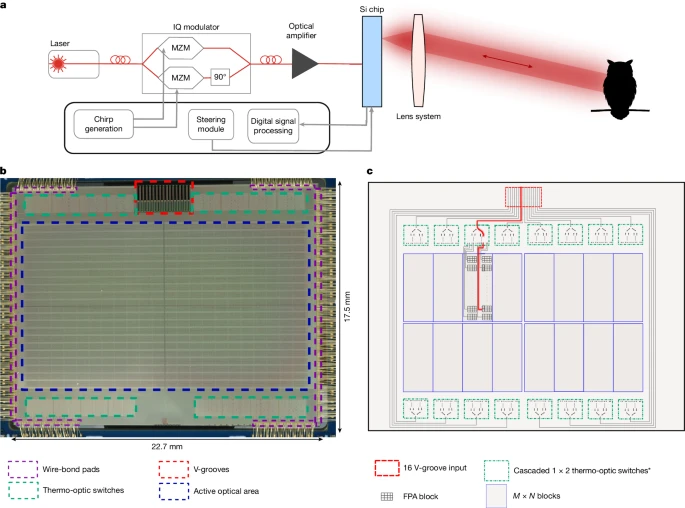
a, The architecture contains an imaging chip that simultaneously functions as both transmitter and receiver. The light path from the chip to target (owl) is determined by the optical lens system. b, Microscope image of the chip, showing the active optical area and thermo-optical switching network. c, Schematic of the light path selection process on the imaging chip. *Some of the outputs of the first-level switches are not connected.
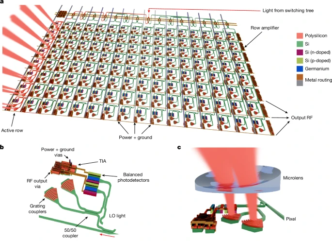
a, Schematic representation of the coherent FPA block. The modulated light is routed to a single 8-pixel row, illuminating a subsection of the scene. The in-plane rotation and emission angle of each grating coupler pair are adjusted to enhance detection efficiency. b, Schematic image of a single coherent pixel, including grating coupler pairs, balanced germanium photodetectors and an integrated TIA. c, Schematic image of a single element of the concave microlens array deposited on-chip to increase light-coupling efficiency.
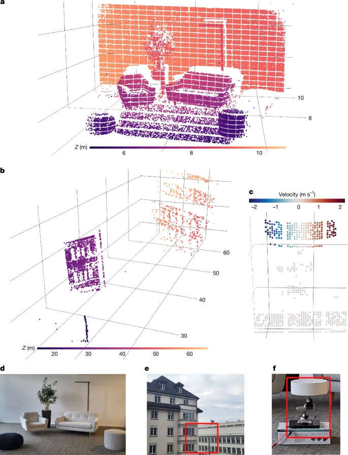
a, Point cloud of an office scene (6–11 m) obtained by a single acquisition using the entire imaging array with a f = 35 mm focal length lens. b, Point cloud from two buildings located 20–65 m away, obtained by coherently averaging four acquisitions with a f = 50 mm focal length lens. c, Velocity-annotated point cloud of the disc that is rotating about its vertical axis, obtained using a single acquisition with a f = 35 mm focal length lens. d–f, Photographs of the scenes in a–c. Red rectangles denote the regions of interest.
Monday, March 09, 2026
Paper on FSI vs BSI for SPADs
In a paper titled "" Eom et al. from Yonsei University, EPFL, Sungkyunkwan University and TruPixel, Inc. write:
This paper presents a process-controlled study of illumination engineering in single-photon avalanche diodes (SPADs) fabricated in a 110 nm standard CMOS image sensor (CIS) technology. Front-illuminated (FI) and back-illuminated (BI) SPADs were implemented with identical front-end-of-line (FEOL) structures, including the junction and guard-ring configurations, enabling the isolation of the effects of illumination direction and back-end-of-line (BEOL) configuration without modifying the junction structure. Through TCAD simulations and comprehensive experimental characterizations, including current–voltage, light-emission, dark count rate (DCR), photon detection probability (PDP), and timing-jitter measurements, we systematically analyze the performance trade-offs introduced by the BI configuration. The BI SPAD exhibits enhanced near-infrared PDP and a broader spectral response due to its deeper absorption region and the incorporation of a metal reflector, while maintaining identical avalanche characteristics, as evidenced by an unchanged 72 ps full-width-at-half-maximum (FWHM) timing jitter. However, the backside illumination increases the diffusion tail, indicating a trade-off between near-infrared sensitivity and diffusion-related timing performance. These results provide design guidelines for optimizing SPAD performance through illumination-direction and BEOL engineering while preserving the FEOL design and demonstrate a useful approach for SPAD integration in standard CMOS technology.
Link: https://www.mdpi.com/1424-8220/26/5/1664
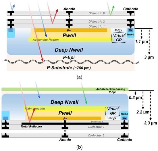
Figure 1. Cross-sections of the SPADs with different illumination configurations: (a) FI SPAD; (b) BI SPAD.
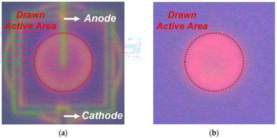
Figure 5. LET results of the SPADs at Vex = 3 V, visualizing avalanche emission across the active area: (a) FI SPAD; (b) BI SPAD.
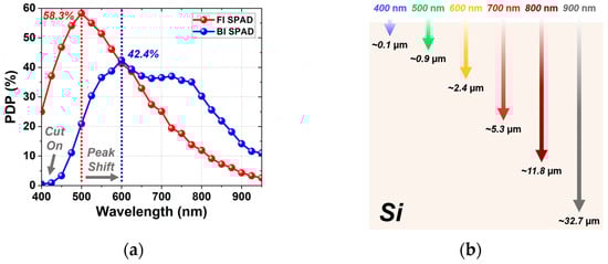
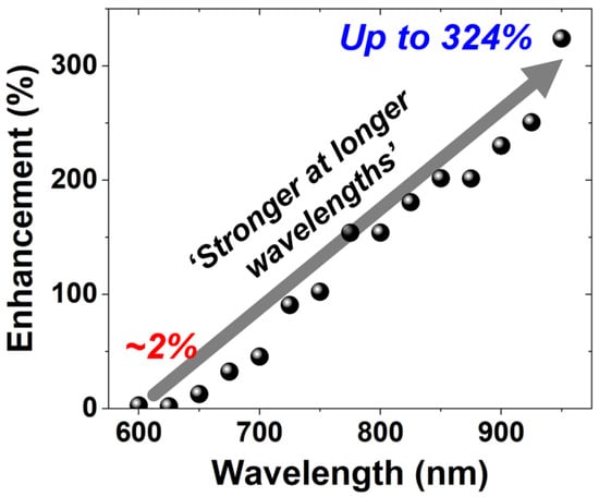
Figure 10. Wavelength-dependent PDP enhancement of the BI SPAD over the FI SPAD.

Thursday, March 05, 2026
Teledyne e2v announces camera with angle-sensitive pixels
From globalnewswire: https://www.globenewswire.com/news-release/2026/03/05/3249875/0/en/Teledyne-e2v-Introduces-Perciva-5D-Camera-Occlusion-free-3D-Vision-for-Industrial-Retail-and-Robotic-Imaging.html
Teledyne e2v Introduces Perciva™ 5D Camera: Occlusion-free 3D Vision for Industrial, Retail, and Robotic Imaging
GRENOBLE, France, March 05, 2026 (GLOBE NEWSWIRE) -- Teledyne e2v, a Teledyne Technologies [NYSE: TDY] company and global innovator of imaging solutions, announces the launch of the Perciva™ 5D camera, a breakthrough imaging innovation designed to make high-quality short-range 3D vision cost-effective, reliable, and easy to integrate.
Most industrial cameras only capture 2D images, yet many applications increasingly require depth perception at close and very-close distances. Perciva 5D delivers this capability through a unique Angular Sensitive Pixel technology and advanced on-board processing, enabling real-time 2D and 3D image fusion at the calibrated working distance range. Perciva 5D also features a powerful Neural Processing Unit (NPU), enabling Artificial Intelligence models to run on-device and be customized to each customer’s specific requirements.
Perciva 5D generates 2D and 3D data from a single CMOS sensor, free from optical occlusion, producing time-aligned 2D frames alongside pixel-aligned 3D depth maps. With comprehensive 3D processing built directly into the camera, users benefit from immediate depth maps or point-cloud outputs. Perciva 5D operates using ambient light, indoors or outdoors, eliminating the need for an external NIR source while maintaining reliable performance and minimizing overall system costs. Designed for challenging environments, it offers plug-and-play integration through its GenICam-compliant, GigE Vision interface and robust IP6x-rated housing with industrial M12 connectors.
Factory calibrated and weighing just 230 grams, Perciva 5D operates at less than 5 W, and is ideal for robotics (arms, cobots and humanoids), retail self-checkout solutions, and 3D industrial process monitoring. It supports user-adjustable frame rates or triggered acquisition and multiple power options. Using GenDC / GenTL the camera integrates seamlessly with Teledyne’s Spinnaker® 4 API and SpinView® for 2D / 3D visualisation, as well as leading machine-vision software platforms.
Perciva 5D will be showcased during Embedded World, Nuremberg, Germany, from 10-12 March 2026. Visit Teledyne at stand 2-541 in Hall 2 or contact us online for more information.
Documentation, samples, and software for evaluation or development are available upon request.
Tuesday, March 03, 2026
New Leadership at Bharat Semi
Dr Boyd Fowler has joined as the Chief Technology Officer at Bharat Semi, an Indian sensor/semiconductor startup.
Here's some text from their recent post:
One of the world's foremost leaders in sensors, Boyd brings deep expertise in CMOS and infrared image sensors, semiconductor architecture, and large-scale engineering strategy. He played a foundational role in developing the technology that enabled commercial image sensors. Additionally, he helped develop the first pinned photodiodes at the world's largest fab. Before joining Bharat Semi, Boyd served as CTO at OMNIVISION Technologies and held senior technology leadership roles at Google, Fairchild Imaging, and BAE Systems. He is known for defining long-term technology vision and leading complex engineering organizations where discipline, scale, and execution are critical.
Link: https://www.bsemis.com/
PS: Bharat Semi should not be confused with Bharath Semiconductors, Bharat Semitech, or Bharat Semiconductor Society.
Subscribe to:
Comments (Atom)