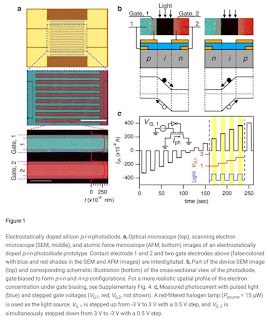
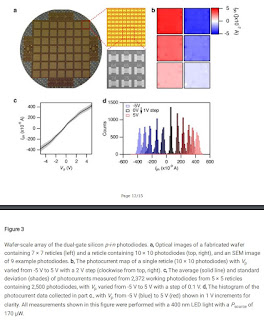
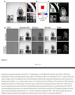
"Complementary metal-oxide-semiconductor (CMOS) image sensors are a visual outpost of many machines that interact with the world. While they presently separate image capture in front-end silicon photodiode arrays from image processing in digital back-ends, efforts to process images within the photodiode array itself are rapidly emerging, in hopes of minimizing the data transfer between sensing and computing, and the associated overhead in energy and bandwidth. Electrical modulation, or programming, of photocurrents is requisite for such in-sensor computing, which was indeed demonstrated with electrostatically doped, but non-silicon, photodiodes. CMOS image sensors are currently incapable of in-sensor computing, as their chemically doped photodiodes cannot produce electrically tunable photocurrents. Here we report in-sensor computing with an array of electrostatically doped silicon p-i-n photodiodes, which is amenable to seamless integration with the rest of the CMOS image sensor electronics. This silicon-based approach could more rapidly bring in-sensor computing to the real world due to its compatibility with the mainstream CMOS electronics industry. Our wafer-scale production of thousands of silicon photodiodes using standard fabrication emphasizes this compatibility. We then demonstrate in-sensor processing of optical images using a variety of convolutional filters electrically programmed into a 3 × 3 network of these photodiodes."
No comments:
Post a Comment
All comments are moderated to avoid spam and personal attacks.