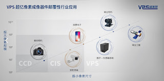
"Perfect fusion of high resolution and large field of view ultra-small pixel size 0.5 micron - ultra-large pixel size of 400 million pixels.
With independent innovation of vertical charge transfer imaging device (VPS) as the core, the company focuses on the development and application design of next-generation ultra-large-scale pixel image sensor chip products, and is committed to providing future-oriented and high-quality imaging performance for medical, commercial satellites and other fields. Large-scale imaging chips and solutions are the leader of billion-pixel imaging chip solutions.
The founding team of the company comes from Nanjing University, Sony, Infineon and other well-known universities and overseas famous chip companies. The R&D team has an average of more than 10 years of industry experience.
The team has completed the research and development and verification of the first chip with a pixel size of 400 million and a pixel size of 0.5 microns. It is the smallest and largest pixel size imaging chip that has been reported. It is mainly used in medical in vitro diagnostics and other fields to help doctors improve diagnosis efficiency , The product is expected to reach 1 billion yuan/year output value within 5 years after the development is completed, and 40+ core intellectual property rights have been applied for.
At present, VPS Vision’s first 600 million pixel imaging chip has begun to be taped out in domestic fabs. This chip has a 0.5 micron pixel size and is known as a digital microchip that can directly "see" cells. It can be revolutionary. To change the existing observation methods, realize the centimeter-level wide field of view and sub-micron resolution simultaneously, and help medical device manufacturers create powerful, cost-effective, and portable devices in the fields of morphology, immunity, and genes, and enter the future for medical equipment."


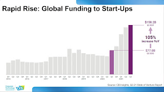
As CES opening talk says, the funding of startups has greatly increased over the past year, so that we can expect more image sensor startups funded:
I heard about this company a few year ago. But I could not find any explanation, e.g. paper, patent... or anything to show us what exactly their 'vertical charge transfer' is. Is it close to what Sony just presented at IEDM? Any one knows?
ReplyDeleteJust to defraud the government.
DeleteIt seems that they have two methods to image by using floating gate.one is like the patant description, another method similar to photo gate,essentially Cis based.
DeleteYou can find some patents info on their website about.
ReplyDeleteE.g. https://patents.google.com/patent/CN102938409A/
Based on the patent, it is completely different from sony's approach, which is still "traditional" 4T. VPS seems to use a memory-based technology, where the charge storage is created with the help of tunneling.
It is quite an interesting idea, but it also reminds me of old news that people tried to make a photo with memory devices.
https://hackaday.com/2014/04/05/taking-pictures-with-a-dram-chip/
If they can get the device in Fig 9 to work well, it would be a small miracle. I expect significant lag and probably low QE, and a lot of FPN and relatively high read noise. So you could demonstrate a few pixels but 100's of megapixels in production seems doubtful without a huge and risky R&D effort. And even then, not sure the advantages are apparent. But maybe this is just a patent app and has nothing to do with the devices they want to bring to market. I applaud the out-of-box thinking but I would not be investing at this time!
DeleteThis patent even has some images. I am still a bit confused about the operation, but it looks like it is a single transistor pixel.
ReplyDeletehttps://patents.google.com/patent/WO2018018762A1/en
How about performance? QE, noise, PRNU, FPN, etc. If they want to convince people their technology works well, they should submit paper to IISW or other top image sensor focused conferences and show real measured data.
ReplyDeleteAny data??? Patent is kind of OK, but patent could be just an idea, it is 'cheap'.
I can only subscribe to this comment. Absolute numbers please.
Delete